
Dot Peen Controller PCB: Plan Power Paths and Copper Weight
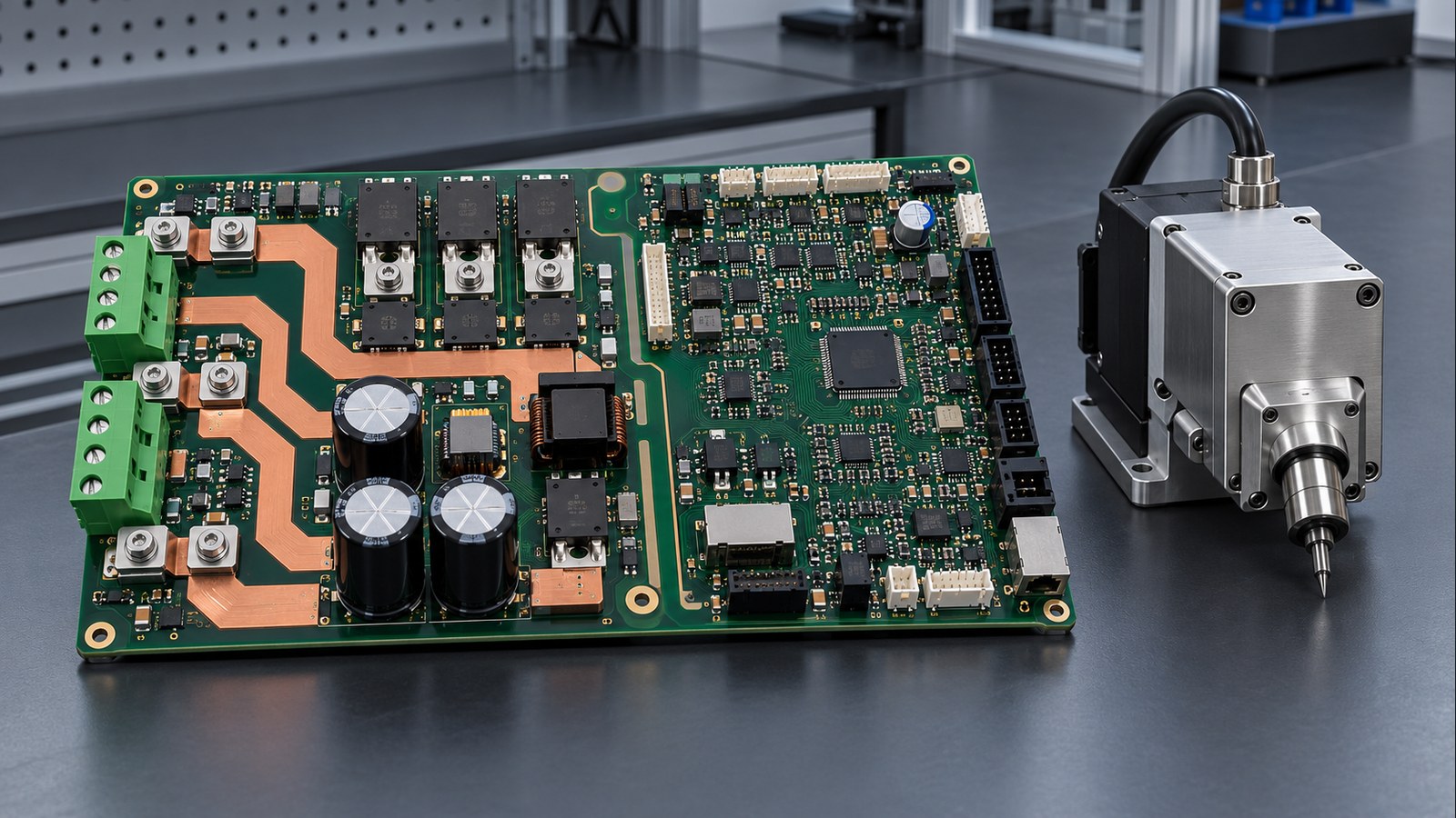
Table of Conent
Table of Conent
Dot Peen Controller PCB: Plan Power Paths and Copper Weight
A dot peen controller PCB should not be assigned a copper weight from the machine’s average current alone. The marking head is a pulsed electromechanical load, so the useful design inputs are peak current, pulse width, duty cycle, simultaneous loads, allowable voltage drop, and the temperature rise permitted inside the enclosure. Start with those waveforms, size each high-current path, and then choose a manufacturable copper stackup. Heavier copper can help, but it does not correct narrow neck-downs, weak vias, undersized connectors, poor return paths, or inadequate transient suppression.
This approach separates the solenoid or actuator energy path from logic, sensing, communications, and safety circuits. It also turns a vague “use 2 oz copper” instruction into requirements that a fabricator and assembler can verify.
Map the current loops before choosing copper weight
The first decision is not trace width. It is identifying every current loop and the conditions under which those loops operate. A typical controller may contain a DC input, reverse-polarity or surge protection, bulk capacitance, a switching stage, a marking-head connector, motor or axis drivers, and low-voltage converters. Draw the forward and return route for each load. The two conductors in a loop must be evaluated together because a wide positive trace with a constricted return still creates loss and heating.
Record continuous current, repetitive peak current, pulse duration, duty cycle, and credible fault current for each path. Include machine states such as homing, head actuation, communication, and auxiliary motion. If the data is incomplete, measure a prototype with current probes at the board input and load connector instead of substituting a fuse rating. Fuse and power-supply ratings are protection limits, not normal conductor design currents.
IPC identifies IPC-2152 as guidance for relating current, conductor size, and acceptable temperature rise. Its charts and modifiers are a starting point, not a substitute for the actual stackup, enclosure, airflow, adjacent copper, and waveform.
Use copper weight and width as one thermal system
Copper weight, finished thickness, trace width, layer position, and nearby planes jointly determine resistance and heat spreading. One ounce per square foot is commonly associated with about 35 µm of starting foil, but finished outer-layer copper can differ after plating and processing. Put the required finished copper thickness on the fabrication drawing and confirm how the supplier interprets it.
For a given route, estimate resistance from resistivity, length, width, and finished thickness. Calculate voltage drop and I²R loss at the relevant current. Then check conductor temperature rise using IPC-2152 methods or a validated simulation. Texas Instruments’ PCB thermal design guidance also emphasizes that copper thickness affects current capacity, thermal behavior, and the stackup. Treat these calculations as design evidence with explicit ambient temperature and cooling assumptions.
A mixed stackup may be more efficient than making every layer heavy copper. High-current outer layers can use wide pours while inner layers support reference planes and signal routing. This choice affects etching, minimum spacing, impedance, via construction, solder-mask registration, and cost, so it should be reviewed early with the PCB supplier.
Find the bottlenecks that copper weight cannot fix
The hottest point is often a local restriction rather than the long straight section of a power pour. Review connector pads, fuse footprints, current-sense resistors, MOSFET drains and sources, thermal-relief spokes, plane splits, and the last few millimeters before the marking-head connector. A broad polygon that narrows at one pad can be limited by that neck-down.
- Define a minimum effective width through every pad transition.
- Use multiple vias for layer changes and evaluate the plated barrel, not only the drill diameter.
- Keep high-current vias away from board edges and mechanically stressed connectors.
- Check connector contact resistance and terminal temperature rise against the actual pulse profile.
- Avoid thermal relief patterns that unintentionally restrict a power connection.
When the design moves from a controller board into a complete machine, the board assumptions should align with the enclosure, cable, head, and acceptance plan. The related dot peen controller box-build acceptance guide explains how those interfaces can be verified together.
Control switching noise at the source
A dot peen actuator produces fast current changes. Keep the switching loop between the local bulk capacitor, driver, protection device, and load connector compact. Place flyback, clamp, or transient-suppression parts according to the driver and load topology. Route the noisy return so it does not share a narrow path with MCU ground, analog sensing, encoder inputs, or communications reference.
Do not split ground reflexively. A poorly placed split can force a signal return around a long detour. Instead, control current paths through component placement, contiguous reference copper, short loops, and deliberate connection points between power and control domains. Validate the result with oscilloscope measurements at the load, gate, logic supply, and communication reference under realistic cable length and repetition rate.
If you want an assembly partner to review the power path before release, send the Gerbers, stackup, schematic, BOM, pick-and-place data, peak-current waveform, cable length, and enclosure conditions through the engineering package submission form. The review can then address fabrication constraints, component sourcing, assembly access, and a practical verification plan rather than copper weight in isolation.
Design the board for assembly and inspection
Heavy copper changes more than electrical performance. Large copper areas draw heat during reflow and hand soldering, while asymmetric copper can contribute to bow or twist. Pad connections around high-current terminals may require a balance between solderability and electrical resistance. Coordinate paste aperture, component thermal mass, selective-solder or hand-solder access, and fixture clearances before production.
The fabrication and assembly documents should state what is controlled. A useful PCB assembly drawing checklist helps capture polarity, special processes, inspection criteria, and test requirements. If multiple head currents or machine options share one board, manage them with an explicit PCB assembly variant plan so the wrong fuse, clamp, shunt, connector, or driver is not loaded.
For a one-stop build, the same release package should cover PCB fabrication, sourced components, SMT and through-hole assembly, programming, inspection, and functional test. The PCB assembly service overview describes the production stages that need to stay aligned with the controller’s electrical assumptions.
Specify evidence, not just a copper number
A purchase drawing that says only “2 oz copper” leaves important questions unanswered. Define the finished copper thickness by layer, minimum conductor width and spacing, stackup, base material, finished board thickness, via requirements, surface finish, and applicable acceptance criteria. IPC’s design standards overview shows how IPC-2152 sits alongside the broader printed-board design standards.
For first articles, request evidence that targets the main risks:
- Measure input and head-current waveforms for the worst operating cycle.
- Record voltage at the supply entry, driver, and marking-head connector.
- Measure temperatures at neck-downs, shunts, drivers, vias, connectors, and bulk capacitors after thermal stabilization.
- Check logic resets, communication errors, and false inputs during repeated marking.
- Inspect solder joints on high-thermal-mass pads and verify programmed options.
Pass/fail limits should come from the product design and component ratings. A thermal image without an agreed ambient, cycle, stabilization time, emissivity method, and limit is useful troubleshooting evidence but not a complete acceptance criterion.
Release checklist for a dot peen controller PCB
Before releasing the design, confirm that the electrical model and manufacturing package agree:
- Peak, continuous, and fault currents are documented for every high-current loop.
- Voltage-drop and conductor-temperature calculations use finished geometry and stated environmental assumptions.
- All neck-downs, vias, pads, fuses, shunts, connectors, and returns meet the same current requirement.
- Switching loops and suppression components follow the selected driver topology.
- Stackup, finished copper, spacing, via construction, surface finish, and inspection requirements are explicit.
- Assembly and test instructions cover variants, programming, functional loading, and thermal verification.
If those inputs are ready, submit the Gerbers, fabrication drawing, assembly drawing, BOM, centroid file, firmware or programming notes, quantities, and test limits through the complete PCBA review intake. That gives engineering and sourcing teams enough context to confirm the stackup, flag bottlenecks, plan assembly, and prepare a quote tied to the real marking cycle.
Conclusion
The reliable way to plan a dot peen controller PCB is to begin with measured current loops and acceptable voltage drop and temperature rise, then choose copper weight and geometry together. Check every local restriction, control the switching loop, and verify the assembled controller under its real duty cycle. This produces a fabrication and assembly package that is easier to quote, inspect, and qualify than a blanket heavy-copper instruction.
Latest Blog
Contact Info
Phone: +86-755-82882936
Email: [email protected]
WhatsApp: +86-13570802455
Wechat: +86-13570802455
Address: 2nd floor,D Bldg.,Electric Link Technology Bldg.,Gongming,Guangming New Dist.,518106 Shenzhen, China