
Vacuum Packer PCBA: Balancing Fine-Pitch SMT and Pin-in-Paste Joints
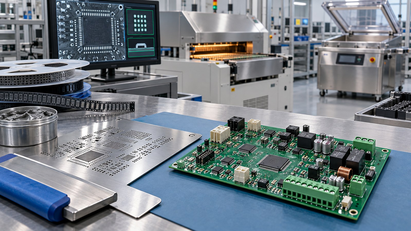
Table of Conent
Table of Conent
A vacuum packer PCBA can combine fine-pitch controllers, small passives, bottom-terminated packages, relays, terminal blocks, and through-hole power connectors on one board. The assembly problem is that fine-pitch SMT usually favors controlled, relatively small paste deposits, while pin-in-paste joints may require much more solder volume to fill plated through holes and form acceptable fillets.
The solution is not a universal stencil thickness. It is a coordinated design that starts with pad and hole geometry, calculates the required deposit for each joint family, checks stencil release and component clearances, selects local step or overprint strategies where justified, and proves the complete thermal process with solder-paste inspection, profiling, first-article inspection, X-ray where useful, and destructive evidence when risk warrants it.
Map the mixed assembly before designing the stencil
Begin with one controlled component and joint map. Identify fine-pitch QFPs, QFNs or other bottom-terminated packages, small chip components, thermal pads, large relays, transformers, terminal blocks, connectors, and every through-hole part proposed for intrusive reflow. Record pitch, land geometry, lead and pin dimensions, hole diameter, board thickness, component body clearance, thermal mass, coplanarity, paste type, and inspection access.
This map should flow into a coordinated PCB assembly process, not remain a design-only worksheet. It determines stencil regions, placement order, support tooling, reflow constraints, secondary soldering, inspection, rework access, and whether a single-pass build is practical.
Confirm that the released fabrication drawing, BOM, placement data, assembly drawings, and component datasheets agree. The PCB design-transfer checklist is useful because a correct stencil cannot rescue mismatched footprints, hole sizes, rotations, or part revisions.
Set fine-pitch deposits from release and joint geometry
Fine-pitch printing requires enough paste to form the joint while releasing consistently from the aperture. Stencil thickness, aperture width and length, wall quality, surface treatment, paste particle size, board support, printer setup, separation speed, and environmental control all influence transfer.
IPC-7525C is the current stencil-design revision listed in the IPC document revision table. Its published table of contents shows coverage of aperture design, area and aspect ratios, fine-pitch technology, step stencils, and intrusive soldering. Those guidelines support engineering decisions, but the final aperture still depends on the actual land, paste, stencil fabrication, printer, and acceptance evidence.
Use aperture reductions, shape changes, window-pane patterns, or local foil changes only for a defined purpose. QFN thermal pads may need divided deposits to control voiding and component float. Fine leads need balanced deposits to reduce bridging and opens. Very small apertures may require thinner foil or improved release conditions, which can conflict with the volume required elsewhere.
Calculate pin-in-paste volume from the finished joint
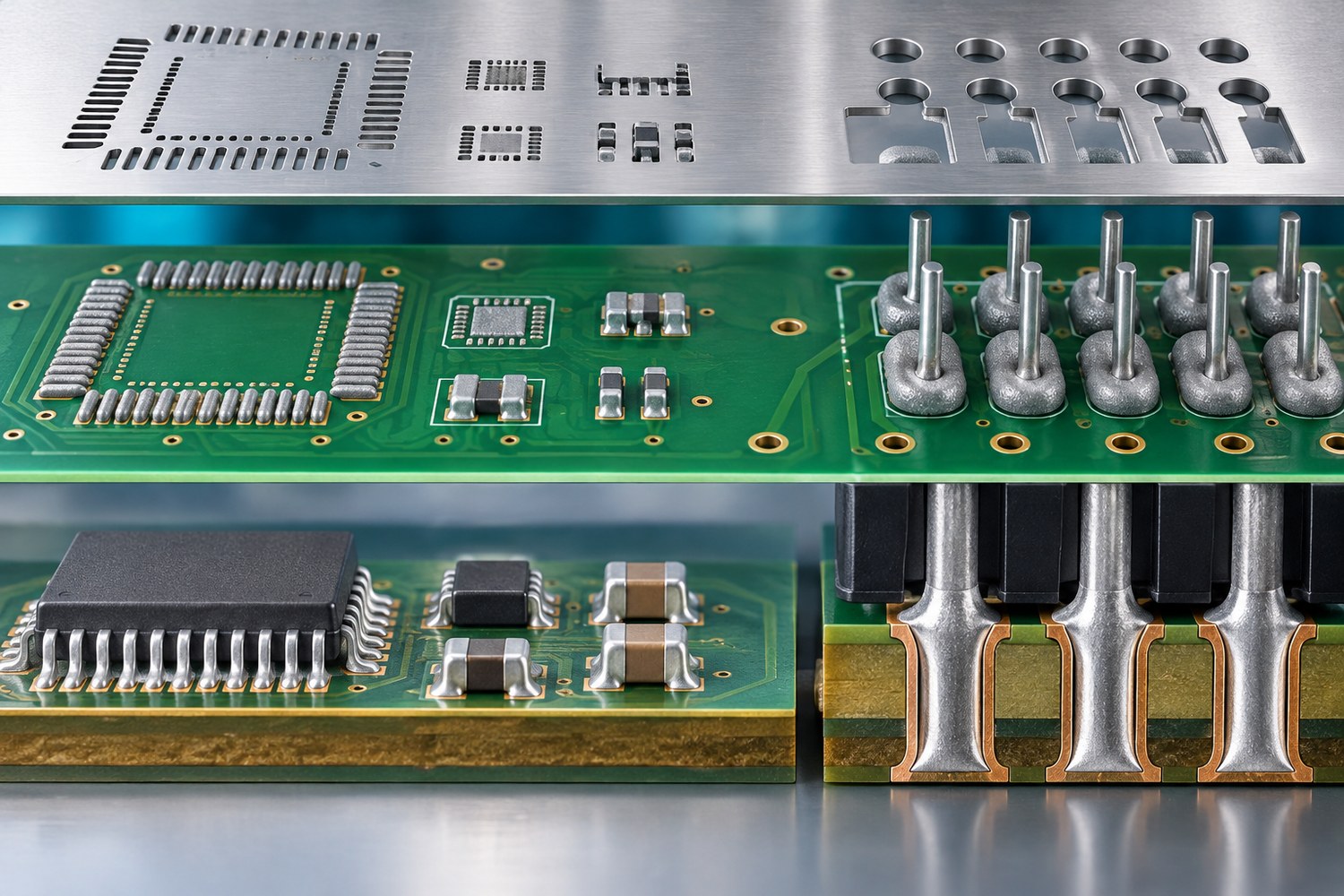
Pin-in-paste, also called intrusive reflow, prints paste over or near a plated through hole before the component is inserted and reflowed with the SMT parts. It can reduce a secondary soldering operation, but it only works when the available paste volume, hole fill, component seating, flux activity, and thermal process are all compatible.
Estimate the solder required from the plated-hole volume, pin displacement, desired fillets, paste metal content, and expected process loss. Then determine whether that paste can be delivered through the stencil without violating nearby clearances or creating deposits that slump, smear, lift the component, or produce solder balls. Overprinting beyond the annular ring, multi-aperture patterns, or a local step-up region may be options when component geometry and spacing allow them.
Not every through-hole part is a good candidate. Verify that the component body, plastic, plating, seal, and internal construction tolerate the full reflow exposure; that insertion does not remove excessive paste; that pins do not block needed outgassing; and that the connector can seat to the intended height. If these conditions cannot be proven, selective soldering, wave soldering, or a controlled hand process may be safer.
Resolve stencil thickness conflicts deliberately
A single uniform foil is attractive, but it may underprint through-hole joints or overprint fine-pitch features. A step stencil can provide thinner regions for fine features and thicker regions for larger deposits, yet it introduces keepout, squeegee travel, cleaning, durability, cost, and printer-setup considerations.
Before selecting a step, model the entire print. Check distance from the step edge to nearby apertures, squeegee direction, board topography, underside gasketing, foil support, paste roll behavior, and whether the chosen printer can reproduce the process. Alternative strategies include overprinting, multiple apertures, preforms, dispensing, or moving selected through-hole parts to a secondary solder process.
If the board and component data are ready, share the Gerber or ODB++ data, BOM, stencil layer, through-hole drawings, quantities, and joint acceptance requirements for a mixed-technology assembly review. The review should expose deposit-volume conflicts and secondary-process assumptions before the stencil is ordered.
Profile reflow for the coldest and hottest locations
The reflow profile must activate the paste and form every joint without exceeding the limits of the board or components. A vacuum packer controller may place high-thermal-mass terminals and relays beside small passives and fine-pitch ICs, creating a wide thermal spread.
Attach thermocouples at representative hot and cold locations: a fine-pitch lead, a bottom-terminated package, a dense ground area, the center of a through-hole connector, and a high-mass power joint. Profile the production-intent panel, support, component load, conveyor speed, and oven recipe. Compare the result with the solder-paste supplier’s process window and every temperature-sensitive component’s documented limits.
IPC’s revision table lists IPC-7530B, released in January 2025, for temperature profiling of mass-soldering processes. A standard can guide the profiling method, but it does not supply the correct recipe for a specific board. The approved profile must be tied to the exact product configuration and monitored for changes in load, oven, fixture, paste, or panel.
Use inspection data to control printing and joint formation
Solder-paste inspection is most useful when it detects process movement before reflow. Define volume, area, height, offset, and bridging limits by feature family rather than forcing one rule onto every aperture. Review trends by board location, aperture type, stencil life, print sequence, and cleaning event.
After reflow, AOI can evaluate visible alignment, fillets, bridges, opens, polarity, and solder balls. X-ray may help with bottom-terminated parts or obscured regions, but it does not automatically establish through-hole fill or mechanical integrity. Cross-sections or controlled destructive analysis may be appropriate during process qualification for high-risk joints.
IPC’s 2024 release notice distinguishes J-STD-001J process requirements from IPC-A-610J assembly acceptance. Purchase and build documents should state the applicable revision, class, addenda, and product-specific criteria. Visual standards do not replace electrical and machine-level functional tests.
Design the board for placement, insertion, and rework
Mixed technology changes the mechanical process. Provide fiducials, panel rails, tooling holes, board support, component-to-edge clearance, insertion access, and a sequence that does not disturb printed deposits. Tall through-hole bodies can block placement heads, interfere with reflow convection, or prevent AOI access if inserted too early.
Define whether through-hole parts are inserted before reflow, after SMT reflow, or in a later cell. Control pin length, clinching, seating force, retention, and component float. Ensure the underside support fixture does not contact paste or components. Plan rework so a damaged connector can be removed without overheating adjacent fine-pitch devices or delaminating the board.
The staged release method in the NPI-to-volume production guide helps contain these risks. Approve stencil data, first print, first placement, profile, first article, and pilot evidence before releasing the full lot.
Verify the controller beyond solder joints
A vacuum packer PCBA must operate pumps, valves, heaters, sensors, motors, safety circuits, communications, and user interfaces as applicable to its design. Production test should begin with safe power-up, rail and current checks, programming identity, configuration, communications, I/O, actuator outputs, sensor simulation, interlocks, watchdog behavior, and fault recovery.
Use representative loads or validated simulators for high-energy or difficult subsystems. Define fixture revision, protection, calibration or verification, software version, expected responses, limits, result format, and failure disposition. The layered controller acceptance framework shows how configuration inspection, wiring checks, controlled power-up, I/O simulation, and functional operation can build evidence safely.
Reliability validation should address the actual thermal, vibration, connector, moisture, cleaning, duty-cycle, and power-transient risks. The board reliability testing method provides a structure for margin, cycling, communication, and recovery tests without inventing universal limits.
Release volume only after the mixed process is stable
The pilot lot should use production-intent PCB fabrication, stencil, paste, components, printer programs, support tooling, placement data, reflow recipe, inspection flow, programming, and functional test. Record paste-inspection trends, defects by joint family, rework, profile results, component seating, hole fill, and functional failures.
Every correction must update a controlled item: stencil revision, aperture data, footprint, hole size, BOM, placement program, work instruction, profile, inspection limit, or test specification. Do not carry pilot fixes into volume through verbal instructions. Establish triggers for stencil replacement, profile reverification, alternate-part qualification, and process reapproval.
When the pilot evidence and release package are complete, provide the fabrication, stencil, assembly, sourcing, programming, inspection, and functional-test requirements for a full PCB assembly evaluation. A useful scope should state which joints use pin-in-paste, which require another process, how acceptance will be demonstrated, and which open risks still need engineering closure.
Conclusion
Fine-pitch SMT and pin-in-paste can coexist on a vacuum packer PCBA when deposit volume, release behavior, component clearance, thermal response, and inspection are engineered together. The goal is not to force every joint through one process; it is to select the simplest repeatable combination that produces acceptable joints without compromising sensitive components.
Map the joint families, calculate rather than guess paste volume, resolve stencil-thickness conflicts deliberately, profile the real assembly, qualify the process on a pilot lot, and connect solder evidence to functional acceptance. That discipline turns a complex mixed-technology board into a controlled production process.
Latest Blog
Contact Info
Phone: +86-755-82882936
Email: [email protected]
WhatsApp: +86-13570802455
Wechat: +86-13570802455
Address: 2nd floor,D Bldg.,Electric Link Technology Bldg.,Gongming,Guangming New Dist.,518106 Shenzhen, China