
Impedance-Controlled PCB RFQ: Define Stackup, Nets, and Acceptance Evidence
Table of Conent
Table of Conent
An impedance-controlled PCB RFQ is quotable when the fabricator can identify every controlled transmission-line class, the intended stackup, the permitted manufacturing adjustments, and the evidence that will constitute acceptance. A note saying only “50 Ω controlled impedance” does not say which traces, layers, reference planes, tolerances, or test structures are involved. The buyer should submit a controlled-net or structure table with the fabrication data, then ask each supplier to return a proposed production stackup and coupon test scope before comparing prices. If the board will also be assembled, the released fabrication revision must travel with the PCBA package.
This is a release framework, not a universal geometry or tolerance prescription. An electrical engineer must choose targets and limits from the actual interface and signal-integrity budget; a fabricator must confirm that the proposed construction can be built and measured. The distinction matters because a passing fabrication coupon supports process control, while the completed channel may include vias, connectors, packages, and other discontinuities outside that coupon.
Describe controlled structures before requesting a price
Give the supplier a controlled-structure list that maps each signal class to a physical construction. A target alone is insufficient: the same nominal impedance can require different trace widths on different layers because dielectric height, copper thickness, reference-plane arrangement, and solder mask change the geometry. Polar Instruments’ controlled-impedance guide describes these dependencies and the trade between conductor width and adjacent dielectric thickness.
In the RFQ table, identify whether a class is single-ended or differential, its target and engineering-approved tolerance, signal layer, reference plane or planes, and the nominal width and pair spacing from the released design. State the units and whether the value applies to the finished board. A named net or class connects the requirement to the design files; a layer number connects it to the stackup. If a class has several neck-down geometries, do not silently pretend a single straight coupon represents every transition.
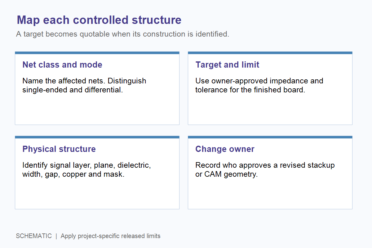
| RFQ field | Decision it enables | Release evidence |
|---|---|---|
| Net or structure class and mode | Distinguishes single-ended traces from differential pairs and groups like geometries | Controlled-net report or marked fabrication drawing |
| Target and tolerance | Defines what the supplier must manufacture and what will pass | Owner-approved electrical requirement with units and revision |
| Signal layer and reference plane | Identifies the dielectric and plane geometry used for the calculation | Released layer map and stackup proposal |
| Nominal width, pair gap, copper, mask | Exposes which physical dimensions may need adjustment | Layout geometry, copper callout, outer-layer mask condition |
| Change and test authority | Prevents an unapproved CAM adjustment or an assumed coupon scope | Named approval owner, coupon class, method and report requirement |
The table is a template, not a claim that one geometry or tolerance fits every board. For a concrete layer arrangement, the 6-layer PCB stackup guide shows how signal and plane assignment affects manufacturability. Boards with denser routing may instead need the options discussed in the 10-layer stackup planning guide. Neither layer count alone defines an impedance acceptance rule.
Freeze the proposed stackup and define who may change it
A comparable quote needs the production construction, not only a design-stage stackup sketch. Send layer order, dielectric material or approved material family, core and prepreg targets where controlled, copper requirements, finished board thickness, and any relevant loss or reliability constraints. Ask the fabricator to return the proposed construction and predicted dimensions for each controlled structure. If the designer has locked a trace width for routing or breakout, say so; if width can move but dielectric thickness cannot, say that instead.
Polar notes that a fabricator can adjust adjacent dielectric thickness when conductor width is fixed, or adjust width when the dielectric is fixed. The feasible choice still depends on the rest of the board and the OEM’s signal-integrity design. Solder resist can change the impedance of a surface microstrip, so identify whether the outer-layer model and acceptance condition include the intended mask. Do not infer that a different laminate with a similar nominal dielectric constant is automatically interchangeable: the design owner should review the relevant material and frequency conditions before approval.
Make the approval boundary explicit. The fabricator may propose a revised stackup or trace geometry during DFM, but the released table and drawing should record who approves the change and what files must be regenerated. In particular, a new width or pair gap may affect spacing, connector escape, and assembly clearances. For a project approaching pilot production, send the controlled-structure table and fabrication files for an engineering scope review; include the quantity and state which dimensions the OEM can or cannot change. The useful next response is a documented stackup proposal and an exception list, rather than an unexplained price.
Specify coupon evidence without claiming it validates the full channel
Decide before quotation whether the supplier will model only, fabricate representative coupons, measure them with TDR, and supply the measured results. These are different deliverables. A coupon should represent the layer, dielectric, copper, mask, and conductor structure being accepted; its design and panel location are manufacturing decisions to agree with the fabricator. Polar’s design-for-test guidance describes why coupon geometry and probe access matter to repeatable testing.
Ask the test report to identify the order or lot, coupon or structure class, target and tolerance, measured value or trace, method and relevant measurement window, and pass/fail decision. The existing PCB impedance testing guide goes deeper into reviewing TDR windows and report quality after fabrication. In this RFQ, the purchasing question comes earlier: whether that evidence is included, how many structures and panels are sampled, and who owns disposition of an out-of-limit result.
| Question | Fabrication evidence | Separate owner decision |
|---|---|---|
| Was the intended geometry built? | Approved production stackup, released artwork and controlled-class record | OEM approves any proposed material, width or stackup deviation |
| Did the representative structure meet the limit? | Coupon design and agreed TDR report tied to the production lot | Buyer defines tolerance, sampling and disposition of failure |
| Will the complete product channel perform? | Coupon result is an input, not full-channel proof | System owner validates vias, connectors, packages and operating interface |
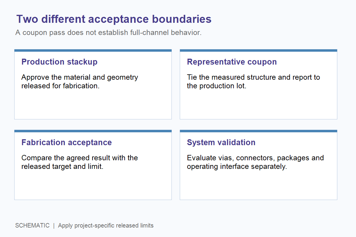
Tektronix’s TDR explanation describes reflections from impedance changes along an interconnect. The measurement method can also reveal launches and transitions, but a straight fabrication coupon does not automatically include every feature in the product channel. Do not turn a coupon pass into an unsupported promise about eye opening, insertion loss, or system behavior.
Connect the fabrication release to assembly without mixing acceptance scopes
If the same supplier or purchasing team coordinates PCB fabrication and PCBA, send one revision-controlled release package to both scopes. The bare-board files define layer order, materials, drill and routing data, finish, and controlled structures. The assembly package adds BOM, placement data, assembly drawings, polarity and programming or test instructions as applicable. A CAM change approved for impedance should be reflected in the released fabrication record before boards enter the assembly lot.
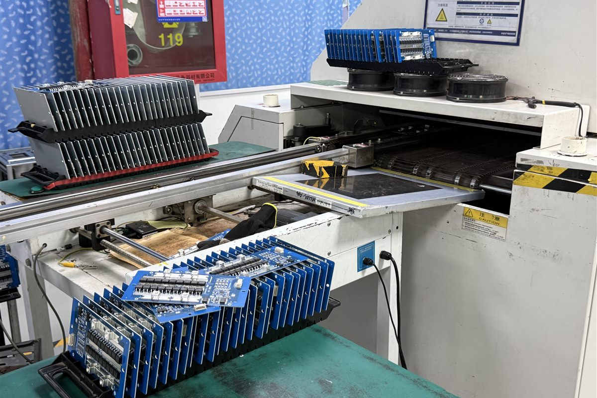
Keep pricing lines distinct: bare-board construction and coupon work, one-time engineering or tooling work, component sourcing, assembly, and board functional test. That makes a price difference actionable. A supplier that includes a measured coupon report and controlled change review is quoting a different scope from one that only accepts artwork and lists a target impedance. The full turnkey PCB assembly service is a route for coordinated fabrication and assembly review; confirm the actual project scope against the submitted release rather than assuming any test or material is automatically included.
Send the RFQ package and compare exceptions, not just totals
A complete request includes fabrication outputs and NC drill files, board outline, layer map, proposed or required stackup, controlled-structure table, material and finish requirements, target quantity, and an explicit coupon and report request. Identify the drawing and BOM revisions. If assembly is in scope, include the placement file, BOM, assembly drawing, and test boundary so the quote covers the handoff as well as the bare board.
OrinewPCB’s short video below outlines the general files that help make a PCB quote accurate. For a controlled-impedance board, add the structure, change-approval, and acceptance detail described above; a generic file checklist alone cannot settle those engineering decisions.
Ask each bidder to mark its proposed stackup, any alternative material or trace geometry, sampling and report deliverables, exclusions, and the approval point for a CAM change. When those items agree, price and lead time become meaningful comparisons. If the release is ready, provide the fabrication package, controlled-net classes, and assembly scope for project review; the response should identify remaining engineering questions and the quote assumptions before production is authorized.
The release test is simple: an engineer should be able to trace each controlled requirement from a net class to a production structure, an approved adjustment rule, and a named acceptance record. Procurement can then compare equivalent work, while the OEM retains responsibility for full-channel performance.
Latest Blog
Contact Info
Phone: +86-755-82882936
Email: [email protected]
WhatsApp: +86-13570802455
Wechat: +86-13570802455
Address: 2nd floor,D Bldg.,Electric Link Technology Bldg.,Gongming,Guangming New Dist.,518106 Shenzhen, China