
Jetson Carrier Board Design: Close Hardware and BSP Interfaces
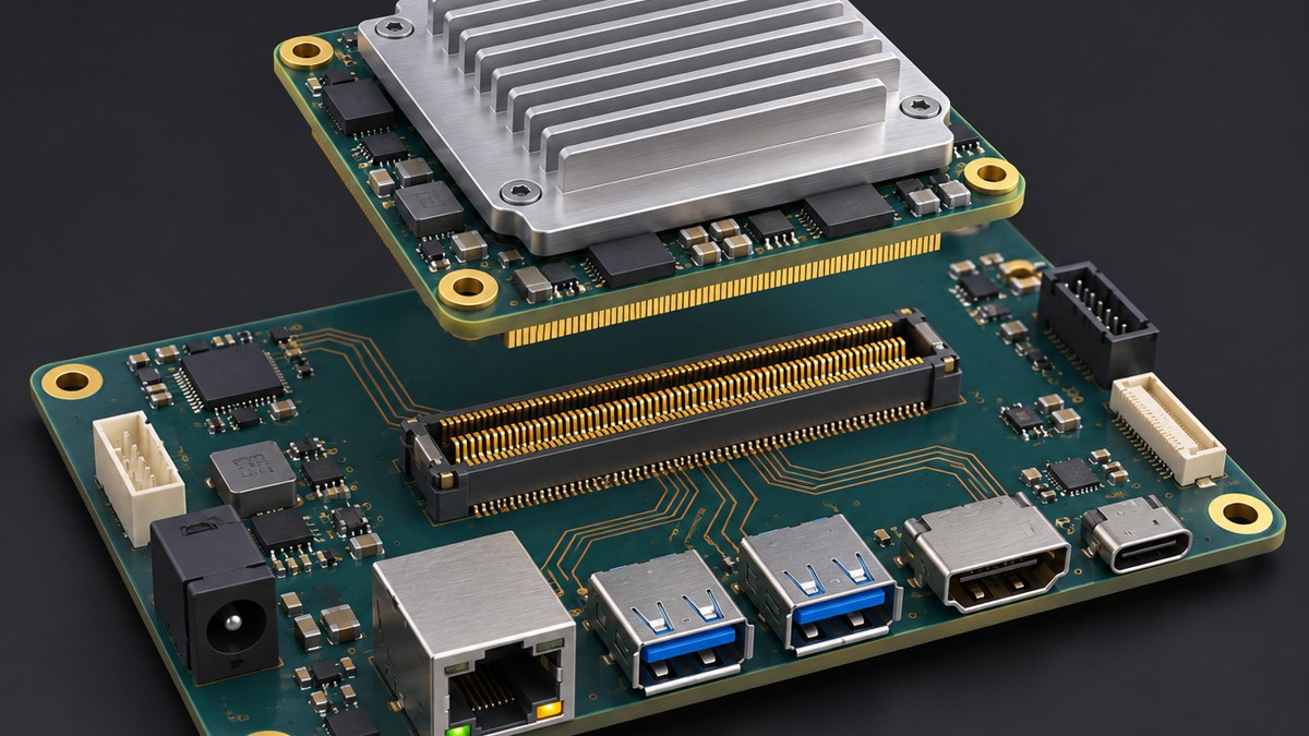
Table of Conent
Table of Conent
A Jetson carrier board is ready for PCB layout when the exact system-on-module, supported interface allocation, power behavior, mechanical envelope and board-support software describe the same product. Choosing a module by compute performance and then copying a development-kit schematic leaves important decisions unresolved. The carrier must connect the intended peripherals, start reliably, provide service access and reject configurations that the released software cannot support. Close those interfaces before paying for the first populated boards.
This guide focuses on a custom edge-computing carrier using Jetson Orin NX or Orin Nano as the working context. Other Jetson families require their own documentation. The system-on-module (SoM) supplies the compute subsystem; the carrier provides application-specific connectivity and supporting circuitry. A board support package (BSP) configures software for that hardware. Release the module part number, carrier revision, BSP version and test package together. Neither a matching connector nor a successful desktop boot proves complete product compatibility.
Freeze the module and software baseline before routing
Use one identified module variant and one supported software release as the design baseline. Treat a proposed module substitution as a compatibility review, even when the outline or connector appears identical. The review should cover the manufacturer’ pin definitions, supported interfaces, power requirements, thermal arrangement, storage and software support. Do not apply a specification from AGX Orin to an Orin NX carrier merely because both names contain Orin.
NVIDIA’ Orin NX and Nano adaptation guide for Jetson Linux r36.4.4 identifies changes to device tree, boot configuration, ODM data and flashing configuration when using a custom carrier. This is a versioned reference, not a claim that r36.4.4 is the latest or correct release for every project. Use the documentation and product design files corresponding to the module and software that the product team actually approves.
Create a configuration manifest with module ordering code, carrier schematic and PCB revisions, BOM, pinmux outputs, device-tree sources, boot configuration and image identifier. Assign an owner to each item. Procurement should know whether the SoM is customer supplied, separately purchased or installed during final assembly. The manufacturing BOM should distinguish the removable module from components soldered to the carrier so sourcing, handling and test responsibilities are priced correctly.
Allocate interfaces as resources, not connector labels
Approve the controller and lane mapping before connector placement. An M.2 socket, USB receptacle or camera connector does not establish that the selected SoM can operate all requested functions together. Record the controller, supported operating mode, physical lanes, associated control signals, voltage domain and software configuration for each implemented interface.
For Orin NX and Nano, NVIDIA documents shared high-speed UPHY resources and specific supported configurations. UPHY is the high-speed physical interface resource beneath the exposed protocols. Use the applicable lane table rather than assigning every desired port independently. A connector-count spreadsheet without this mapping can conceal a conflict until bring-up. Resolve unused pins and interfaces intentionally, following the product design guide rather than borrowing termination or pull settings from another carrier.
| Interface decision | Record before layout | Evidence before pilot acceptance |
|---|---|---|
| PCIe storage or expansion | Controller, supported lane grouping and mode, clock and reset relationship | Endpoint identification and defined transfer test on the released image |
| USB connection | Port mapping, host/device role, power switching and protection | Intended peripheral operation and recovery access where assigned |
| Camera connection | Sensor, interface mapping, control bus and software driver ownership | Image capture under the specified sensor mode |
| Low-speed control | Pin function, voltage, pull state and startup behavior | Observed levels and functional operation in relevant states |
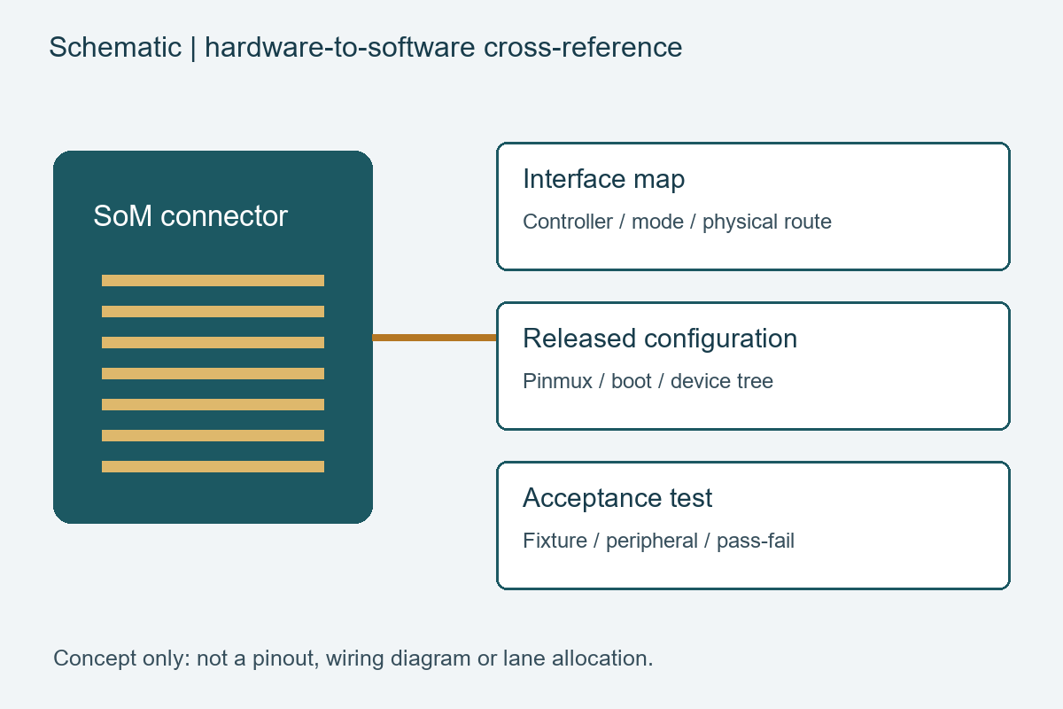
Keep a schematic-to-software cross-reference beside this map. For example, a changed reset net may require both a hardware change and a device-tree update. A pin that works after an interactive debug command still needs a reproducible production configuration. Ask the software owner to approve the generated settings and flashing inputs before the board is released.
Once the map is coherent, a manufacturing team can assess the carrier’ fabrication and assembly constraints. If that review is needed, share the carrier files and interface constraints with the BOM, pilot quantity and module-supply boundary. The next step is to align fabrication, sourcing, assembly and test scope with the released design; BSP development should be assigned explicitly rather than assumed to be included.
Close power, thermal and high-speed layout together
Design the carrier for the selected operating conditions and the whole connected system. A module power-mode label is not a complete input-supply budget: peripherals, conversion losses, startup behavior and allowed transients also matter. Use the exact module design guide for sequencing and electrical limits. Define which rails are measured, where they are measured and which load states must be exercised.
Thermal acceptance should name the enclosure, cooling solution, ambient condition and representative workload. NVIDIA’ versioned power and performance documentation describes power-mode and thermal management behavior. A short idle boot test cannot replace sustained workload evaluation in the intended mechanical assembly. Specify the observation period and acceptable behavior for the actual application rather than publishing a universal heatsink size or temperature limit.
Place the module connector, mounting points, thermal hardware and external connectors together in the mechanical review. Check insertion clearance, retention, service access and the keepouts required by the component drawings. A cooling bracket that fits the standalone PCB may interfere with a cable or obstruct access to a recovery connector after enclosure assembly. Resolve these constraints while the placement can still move.
For high-speed nets, release the target stackup and interface-specific routing constraints with the fabricator. Trace width alone does not specify impedance: reference planes, dielectric construction, copper and the complete route matter. The controlled-impedance fabrication package should identify the relevant nets and acceptance evidence. Avoid a universal layer count or trace-width recipe for every Jetson carrier; connector density and the implemented interfaces determine the actual construction.
Make recovery and fault isolation accessible on the pilot
Preserve a documented way to recover and diagnose an assembled unit. Decide how the technician reaches recovery controls, the required USB connection, debug UART and key power measurement points. Confirm access with the module, heatsink and enclosure installed. A recovery pad hidden under the finished assembly converts a routine software recovery into mechanical rework.
Build a staged acceptance procedure: inspect the unpowered assembly, verify the approved power behavior, establish recovery and flashing, check boot logs, then exercise each implemented interface. Add the defined workload and thermal checks after basic functions are established. NVIDIA’ hardware and software bring-up checklists provide review prompts; follow their applicability markings and the selected module’ requirements, not every numeric example in a generic checklist.
Separate a population defect from a configuration mismatch before changing either the BOM or software. Compare a failing pilot with a known-good unit using the same module variant, image, peripherals and cables. Capture the observed failure and the gate at which it appears. Changing the power circuit and flashing a different image at the same time removes the evidence needed to determine which change helped.
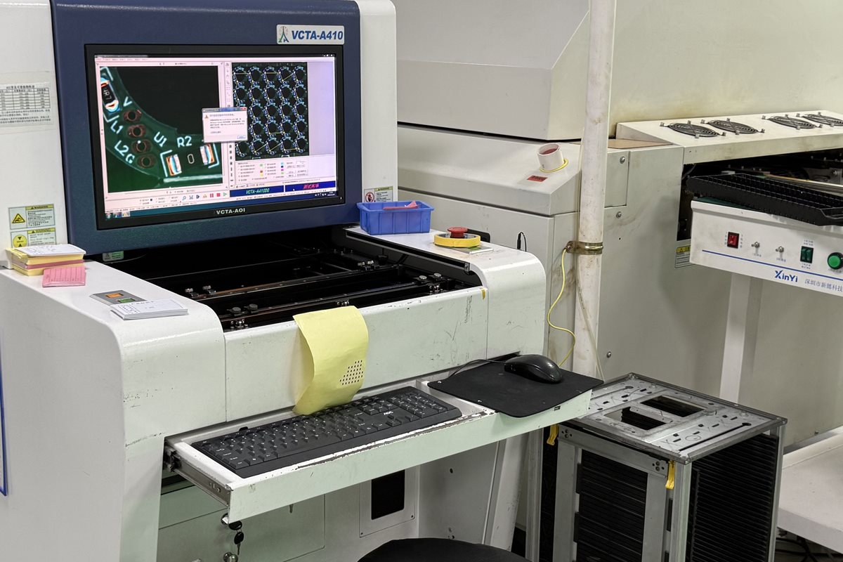
Optical inspection can establish visible assembly features within its inspection scope. It cannot verify lane configuration, a complete camera path or recovery behavior by itself. The requirement-to-test acceptance record should assign these checks separately and link the result to the carrier revision and image identifier.
Transfer a repeatable build, image and acceptance package
Release production only when another operator can build and test the same configuration from controlled instructions. Include fabrication data, stackup, BOM, approved alternates, placement and assembly drawings, module handling, thermal hardware, flashing inputs, test software and acceptance limits. State what the supplier ships: a populated carrier, a module-installed assembly or a tested enclosed product.
| Boundary | Controlled input | Returned evidence |
|---|---|---|
| Fabrication and population | PCB/BOM revisions, approved parts and assembly drawing | Build identification, inspection and approved deviations |
| Software configuration | Module compatibility list, image and flashing procedure | Image identifier and programming result |
| Interface function | Port map, fixtures, peripherals and pass/fail criteria | Unit-linked results for implemented functions |
| Mechanical and thermal integration | Retention, cooling arrangement and workload conditions | Fit checks and required system test records |
Compare quotations against these boundaries rather than carrier assembly price alone. Confirm who supplies the module and test peripherals, who maintains the production image, and who approves substitutions. The full-turnkey PCB assembly scope provides a manufacturing framework; custom Jetson BSP engineering and application validation still require explicit agreement.
A sound release connects the exact SoM to a feasible interface map, a compatible software configuration and repeatable acceptance evidence. For a project ready to proceed, provide the controlled carrier and assembly package with quantities, module ownership and the test responsibilities. This lets fabrication, component sourcing, assembly and any agreed programming or testing be evaluated as one defined project.
Latest Blog
Contact Info
Phone: +86-755-82882936
Email: [email protected]
WhatsApp: +86-13570802455
Wechat: +86-13570802455
Address: 2nd floor,D Bldg.,Electric Link Technology Bldg.,Gongming,Guangming New Dist.,518106 Shenzhen, China
