
Radio Altimeter PCB Thermal Design: Control the Heat Path
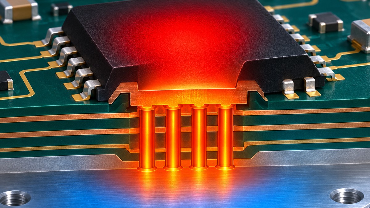
Table of Conent
Table of Conent
A radio-altimeter PCB needs a controlled heat path and a repeatable RF test boundary before it can support an equipment qualification program. Start with the actual component losses, the enclosure and mounting arrangement, the selected environmental conditions, and the electrical limits that must remain satisfied at those conditions. A cooler board surface alone does not prove an acceptable junction temperature or stable RF performance. Likewise, a board that passes assembly inspection is not automatically a DO-160-qualified radio-altimeter system.
This article addresses thermal design and manufacturing handoff for the board inside an airborne radio altimeter. It does not supply a flight installation design or universal acceptance limits. The OEM and responsible approval organization must select the applicable requirements and test configuration. The practical manufacturing objective is narrower: build the released thermal interfaces consistently, identify changes that affect them, and return evidence that the specified board and equipment tests actually used the intended configuration.
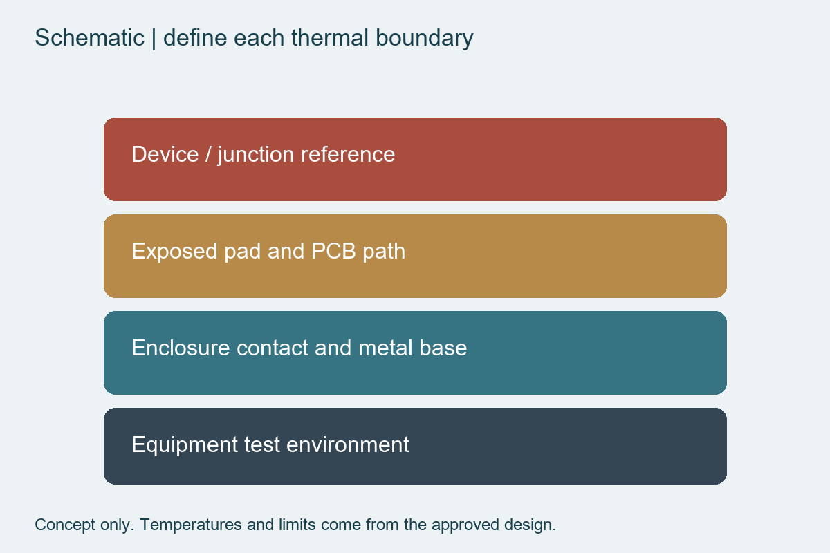
Define the thermal boundary before selecting the board construction
Release a heat-flow budget for the assembled equipment, not just a list of component maximum temperatures. Identify the dissipating devices, their operating states, the receiving structure for the heat, and the conditions at which the design must work. Regulators, digital processing and RF components can create different local temperatures even when they occupy one small board.
For each significant device, distinguish electrical input power from the heat dissipated inside the package. Use the component documentation and the intended operating point. Then identify the relevant thermal metric and reference temperature. A junction-to-case value cannot simply be treated as junction-to-ambient resistance. Analog Devices’ AN-2591 discussion of RF amplifier junction temperature explains why dissipation, thermal resistance and the relevant temperature boundary must be considered together. Its package-specific discussion is useful engineering context, not a qualification limit for every radio-altimeter component.
The enclosure belongs in this budget. Record whether the board transfers heat through mounting hardware, a baseplate, a heat spreader, an interface pad or another defined route. Include the mechanical tolerances that determine contact. An open-bench prototype can have a different heat path from the same populated PCB inside its production enclosure. The pilot test should expose that difference before purchasing commits to a volume build.
Specify the exposed-pad and enclosure interfaces as manufacturing features
A thermal path is only useful if the assembled product can reproduce it. For components designed to conduct heat through an exposed pad, the pad pattern, solder connection, PCB structure and downstream mechanical interface all need controlled definitions. Use the exact component land pattern and assembly recommendations; a generic via array should not replace them.
Analog Devices’ AN-1604 thermal-path modeling method treats the PCB and attachment to the heat sink as parts of the RF amplifier heat-flow path. The manufacturing implication is to identify each relevant interface in the release package. Ask whether the fabrication drawing specifies the intended via construction, whether solder processing can achieve the approved pad connection, and whether the enclosure assembly maintains the intended contact condition.
| Interface | Controlled input | Evidence to agree before the build |
|---|---|---|
| Device to PCB | Approved package land pattern and solder process requirements | Applicable inspection method and acceptance criteria |
| Heat transfer through PCB | Stackup, relevant copper and via construction | Fabrication records and specified verification |
| PCB to enclosure | Contact location, interface material, thickness or fit requirement | Assembly and dimensional checks |
| Equipment to installation | Mounting and environmental boundary selected by the OEM | Equipment test configuration and applicable reports |
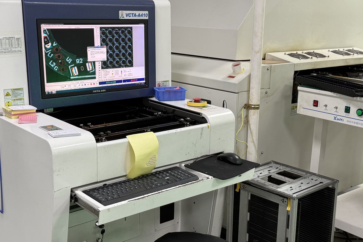
Specify the inspection method and acceptance criteria for a hidden thermal pad rather than requesting that it simply look good. Optical inspection cannot establish the complete concealed solder connection. If radiographic inspection or another method is required, define its purpose and the applicable acceptance rule in the purchase package. Do not invent a universal void percentage: the relevant package guidance and program requirements must establish the limit.
After the interfaces are defined, teams can share the thermal-interface drawings and assembly constraints with the BOM, fabrication files and pilot quantity. This allows the manufacturing review to address PCB construction, component sourcing, solder processing, mechanical integration and agreed inspection together. Identify any thermal or RF test that remains with the OEM so it is not silently assumed to be included.
Review thermal changes against the RF construction
Approve a thermal change only after identifying the electrical features it may affect. Adding copper, changing a laminate, altering via construction or attaching metal near an RF region can change more than temperature. The correct decision requires the released RF geometry and component application information, followed by the agreed verification.
Use the controlled-impedance fabrication requirements to name critical nets, reference planes, stackup and acceptance evidence. Keep the heat-flow route and RF return-current route visible in the same review. A useful thermal feature can be unacceptable if it disrupts the intended electrical construction. Conversely, preserving a nominal trace width while changing the underlying construction does not preserve all RF behavior.
Laminate selection needs separate questions for thermal reliability and heat removal. Glass transition temperature, or Tg, describes a resin transition; it is not itself thermal conductivity or a complete continuous-use temperature rating. A higher-Tg label alone therefore cannot establish a lower component junction temperature. Obtain the properties needed for the actual electrical, thermal and assembly decisions and evaluate the proposed material as a controlled change.
The official OrinewPCB short below introduces the distinction between standard and high-Tg FR-4 as a material-selection topic. It is AI-generated educational content, not radio-altimeter qualification evidence or a measurement of this board’s thermal performance.
Test RF behavior at the released thermal condition
A thermal acceptance test should pair a defined configuration with the measurements needed to assess it. Record the board revision, components, firmware where relevant, enclosure, interface material, mounting arrangement, operating mode and instrumentation. Name the temperature reference and the equipment state. Without those details, a later build cannot reproduce the result or establish whether a changed interface is equivalent.
The OEM should define which RF or functional limits must be checked at each required condition. Possible categories include gain, frequency behavior, noise or complete functional output, depending on the architecture and approved procedure. This is a planning menu, not a universal radio-altimeter test specification. Define the measurement reference planes, cable treatment, instruments, test software and applicable pass/fail criteria before asking the supplier to price the test.
Use the requirement-to-test acceptance record to connect each decision to evidence. A board temperature reading answers a thermal question at that location. An RF test answers its specified electrical question under its stated conditions. An assembly image answers an inspection question. Keep those records distinct so one successful result is not used to imply that all three questions have been answered.
RTCA describes DO-160 environmental conditions and test procedures for airborne equipment. The project must select the applicable edition, categories and acceptance conditions; this article does not derive those from a generic PCB label. A chamber test with an undefined mounting arrangement or an unrepresentative operating state can leave the intended equipment boundary untested.
Release changes and qualification evidence at the correct level
The production release should connect every thermally significant feature to a controlled drawing, process or acceptance requirement. Include the fabrication and assembly revisions, BOM and alternate rules, interface material, mechanical instructions, test configuration and deviation procedure. Define which changes require review and which measurements must be repeated.
| Proposed change | Review question | Evidence selected by the responsible engineer |
|---|---|---|
| Laminate or stackup | Does the heat path or RF construction change? | Material comparison and affected electrical/thermal verification |
| Exposed-pad assembly process | Is the approved attachment condition maintained? | Applicable process and inspection evidence |
| Interface pad or enclosure fit | Is the intended contact reproduced? | Fit checks and affected temperature/function tests |
| Component alternate | Do losses, package or RF behavior differ? | Engineering approval and relevant regression tests |
Separate manufacturing acceptance from equipment and installation approval. FAA AC 20-199 on radio-altimeter system installation, issued July 24, 2026, addresses a system including the transceiver, antennas, cabling and displays or indicators. That scope reinforces why a bare board or a single thermal result cannot establish approval of the installed system.
The full-turnkey PCB assembly scope can support a coordinated manufacturing review, while radio-altimeter-specific limits and qualification responsibility must remain explicit. The release decision is to control the complete heat path, verify relevant RF behavior at the selected conditions, and preserve the resulting configuration through production.
For a project ready for manufacturing evaluation, provide the controlled board and equipment-interface package with the BOM, quantities, assembly data and test ownership. The team can then assess fabrication, sourcing, assembly and any agreed mechanical or test work against the same requirements rather than an unsupported claim of a qualified PCB.
Latest Blog

Contact Info
Phone: +86-755-82882936
Email: [email protected]
WhatsApp: +86-13570802455
Wechat: +86-13570802455
Address: 2nd floor,D Bldg.,Electric Link Technology Bldg.,Gongming,Guangming New Dist.,518106 Shenzhen, China
