
PCB Aspect Ratio: Drill Diameter, Depth, and Fabrication Review
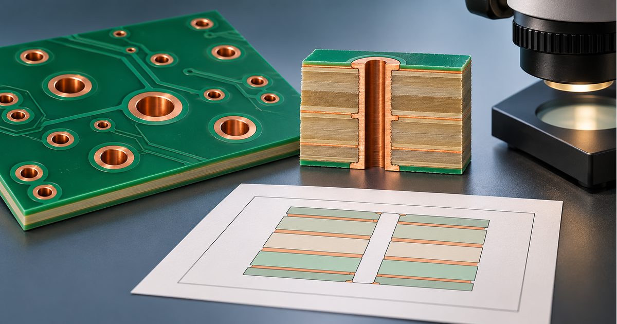
Table of Conent
Table of Conent
PCB aspect ratio describes how deep a hole is relative to its diameter. It is an important fabrication check because a deep, narrow opening presents different drilling and plating demands from a shallow, wide one. The ratio helps frame a supplier discussion, but it does not by itself establish that a board is manufacturable or reliable.
A meaningful review needs the hole type, actual depth, diameter basis, stackup, and applicable process requirements. Two drawings can show the same finished opening while implying different production geometries. This guide explains how to calculate the ratio consistently, compare design alternatives, and prepare the evidence needed for an engineering and purchasing decision.
State the calculation convention before comparing numbers
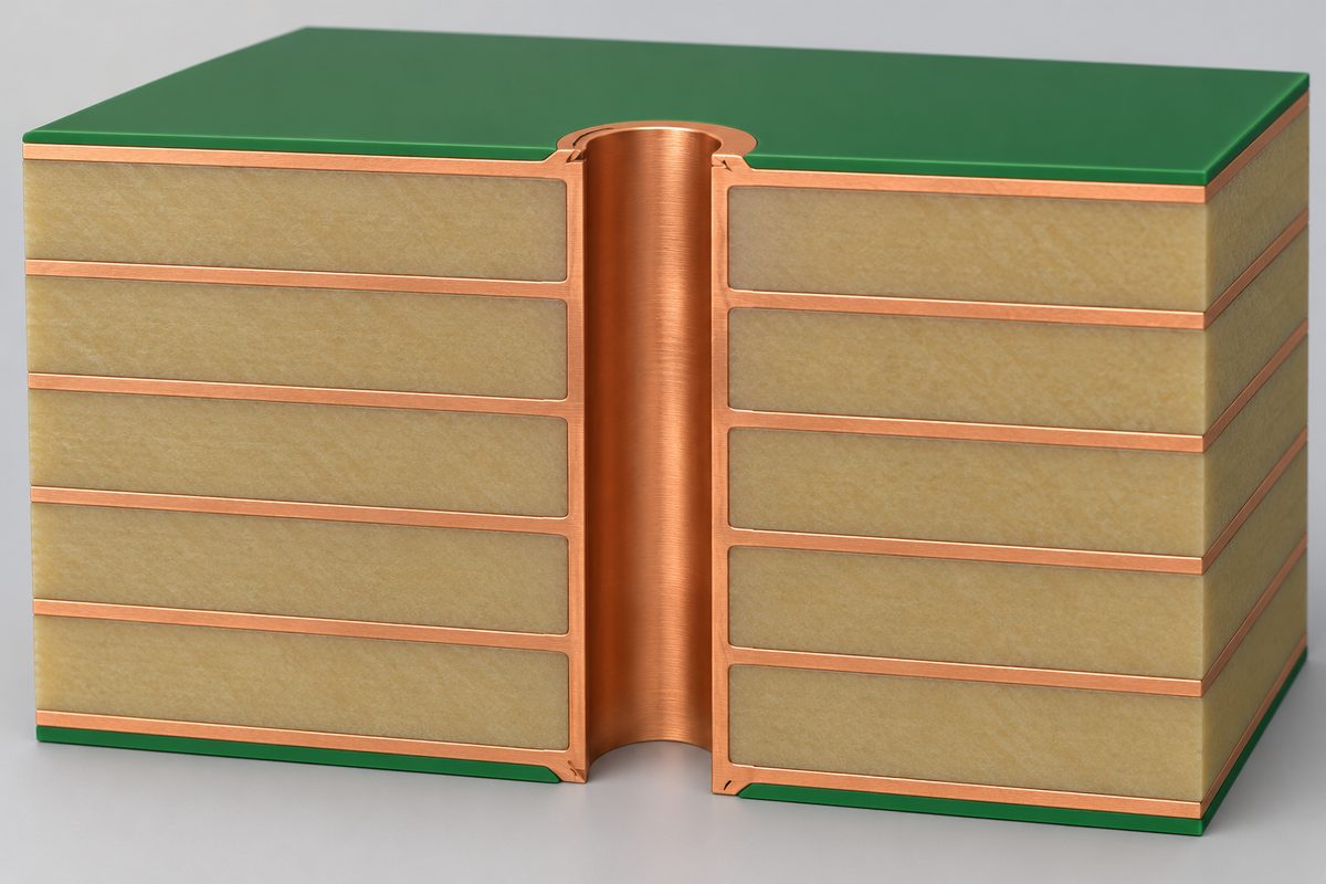
In this article, aspect ratio means hole depth divided by the applicable drilled-hole diameter. Both quantities must use the same units. The result is dimensionless and can be written as a ratio, such as 6:1.
For a mechanically drilled through hole, depth ordinarily spans the board construction through which the hole is formed. For a blind or buried structure, the relevant depth is the material span involved in that hole’s fabrication, not automatically the final board thickness. Confirm the supplier’s definition rather than assuming every capability table uses identical inputs.
JLCPCB’s via aspect-ratio explanation uses drilled diameter before plating. That distinction matters because the finished opening is smaller after material is deposited on the walls. Its capability examples are specific to its discussion; they are not AssyPCB limits or acceptance criteria.
When a drawing specifies a finished hole, keep that requirement intact. Ask the fabricator to identify the production diameter used in its assessment. Do not invent a fixed drill allowance or overwrite component-fit requirements to make a calculated ratio look better.
Use examples to understand the direction of change
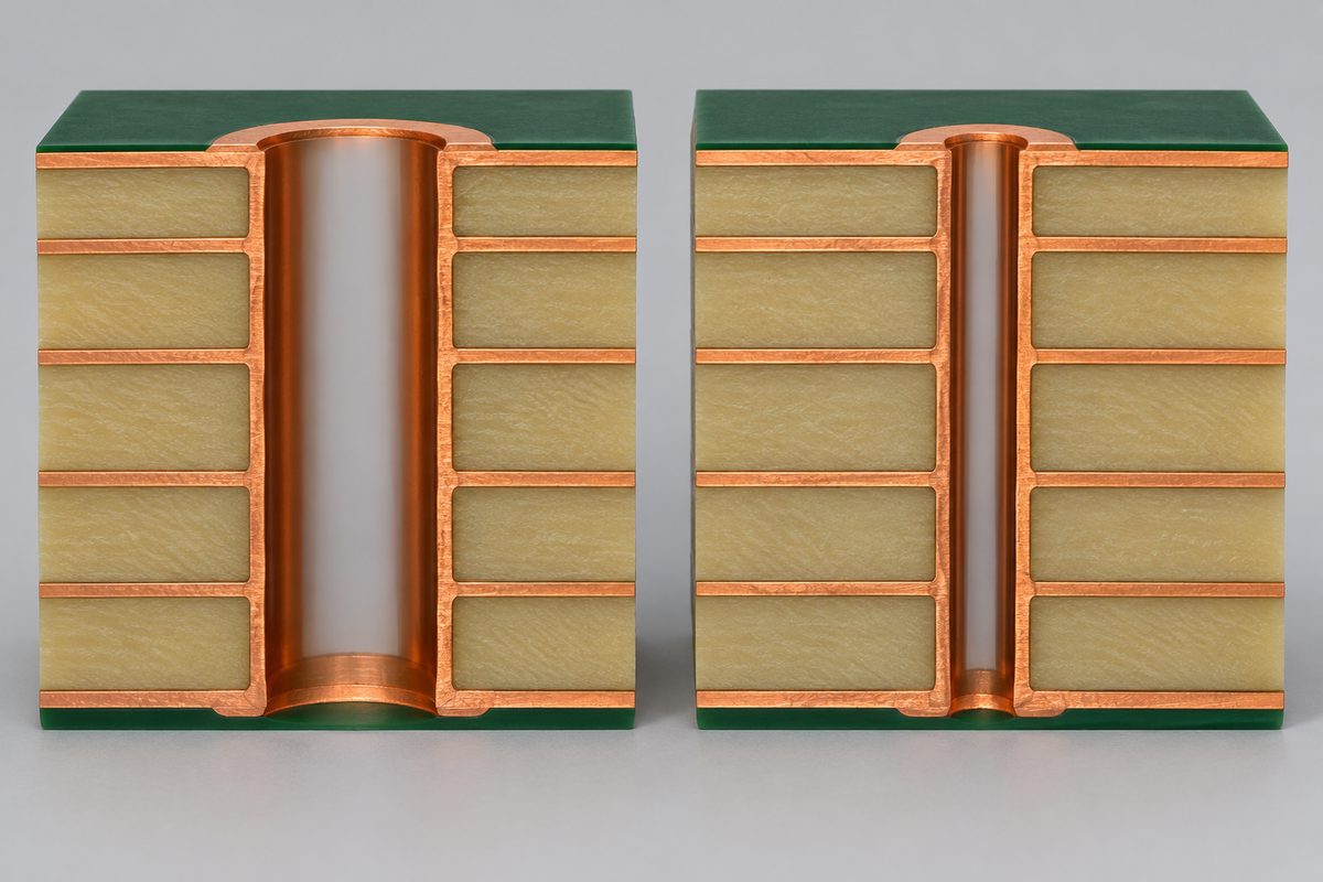
Consider a hypothetical drilled opening with a depth of 1.80 mm and a diameter of 0.30 mm. Its aspect ratio under the stated convention is 1.80 / 0.30 = 6:1. These are illustrative dimensions, not an approved stackup or recommended via size.
If the depth stays at 1.80 mm but the diameter becomes 0.20 mm, the ratio becomes 9:1. If the diameter remains 0.30 mm and the depth increases to 2.40 mm, the ratio becomes 8:1. A smaller denominator or larger numerator increases the ratio; the drawing must make clear which quantity changed.
For a tolerance-sensitive assessment, nominal dimensions alone may not be sufficient. Ask how depth variation and the relevant hole-size variation enter the supplier’s review. Do not substitute a finished-hole tolerance directly for tool variation or add tolerances already included in a stated process allowance.
Record the calculation inputs beside the result. A spreadsheet cell labeled only “9:1” is difficult to audit if nobody knows whether it used total board thickness, a local dielectric span, a nominal drill, or a finished opening.
Why the ratio matters to fabrication
A narrow opening extending through a thicker construction is more demanding to process consistently. Hole preparation and copper deposition must reach the relevant surfaces through that geometry. Insufficient coverage or unsuitable processing can undermine the intended connection, even when the layout appears electrically complete.
The ratio is therefore a screening parameter, not a complete quality model. Material construction, hole preparation, plating requirements, and the selected process also matter. A larger permitted ratio in a capability table does not mean every material and copper requirement can be combined at that limit.
Siemens’ aspect-ratio DFM discussion highlights the need to communicate thickness information as well as hole data to the manufacturer. A drill file can identify openings without providing the full construction needed to judge their depth.
Ask whether a quoted limit is a routine production recommendation, a conditional maximum, or a value requiring a specific process review. Also identify which hole construction it covers. These questions are more useful than choosing the highest published number and designing every via to match it.
Separate through holes from partial-depth structures
A through hole and a partial-depth hole should not be assessed as if they have the same depth just because they share a nominal diameter. For a buried structure, the relevant manufacturing span may belong to a subassembly that is later incorporated into the final board.
Blind vias and laser-formed microvias also introduce construction-specific geometry and processing. A ratio rule developed for a mechanically drilled through hole should not be transferred automatically to them. Discuss the layer span, opening definition, fill or cap requirements where applicable, and the proposed build sequence.
Changing the via architecture can shorten the relevant depth, but it may add manufacturing steps and change routing or reliability requirements. It is not a free substitution. Confirm the feasible construction before routing a dense region around an assumed alternative.
If the intended hole span is unclear, send the proposed stackup, layer-pair definitions, drill data, and via construction notes for an engineering and quotation review. Identify the holes driving the decision so the supplier can assess a concrete configuration.
Compare changes without ignoring their side effects
Increasing drill diameter reduces the calculated ratio at a given depth, but it can require larger lands and alter spacing around the hole. Check the routing channels, copper clearances, plane isolation, and relevant assembly footprint after the change. A lower ratio is not a sufficient reason to accept a new clearance violation.
Reducing board thickness can also reduce through-hole depth. However, thickness may be constrained by connectors, mechanical fit, stiffness, copper construction, or electrical requirements. Our PCB thickness selection guide explains why those constraints should be considered together rather than changing thickness solely to improve one calculation.
Changing hole type is a third option, but it requires confirmation of the layer span and fabrication sequence. Compare options with the same required function: electrical connection, component fit, or mechanical attachment. Do not quietly change a component hole into a different via construction.
For a hypothetical design tradeoff, a larger through-hole via might preserve the existing stackup but consume more routing area. A partial-depth alternative might retain more routing space while requiring a different build. The preferred option depends on the actual design and confirmed quotation, not a universal ranking of technologies.
Use the PCB manufacturing capabilities page to start the discussion, then confirm the complete combination of thickness, material, hole diameter, and required plating for the order. Do not read isolated capability entries as approval of every possible combination.
Prepare a hole-family review instead of one board-wide number
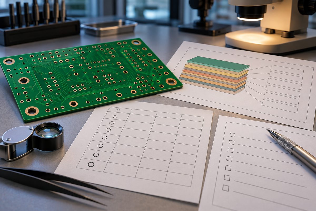
A board can contain multiple hole families with different diameters, functions, and spans. Group them explicitly. Identify through-hole vias, component holes, and any partial-depth structures separately. The smallest finished opening is not necessarily enough information to identify the most demanding production feature.
For each family, record its reference or location, plated status, depth basis, diameter basis, proposed ratio, and applicable requirements. Mark the data that remains subject to supplier confirmation. A concise list is easier to review than scattered notes across several drawing revisions.
Keep the released drill, copper, stackup, and fabrication drawing revisions aligned. If a supplier proposes a change, document the revised input and rerun the dependent layout checks. A ratio calculated from an older stackup cannot approve a new one.
Where a hole family approaches a confirmed process boundary, request a review with the hole-family list, critical requirements, and acceptable design alternatives. Ask for a response tied to the submitted revision rather than an informal statement that a similar board was manufactured before.
Agree on evidence as well as design limits
Fabrication review and acceptance evidence serve different purposes. A favorable ratio check does not measure the copper in the finished holes. Likewise, an electrical continuity result does not establish plating thickness or prove performance under every later thermal exposure.
Eurocircuits’ microsection overview illustrates how sectioned samples can examine internal connections and through-hole plating. Its sampling routine is its own practice, not an AssyPCB promise. Agree on the evidence and applicable criteria required for your project before production.
Our PCB microsection analysis guide provides context for sample identification and interpreting the location examined. A section is evidence about the sampled feature; it should not be presented as a direct measurement of every hole in the shipment.
Release review checklist
- State the aspect-ratio convention and use consistent units.
- Identify each relevant hole family and its manufacturing span.
- Distinguish drilled dimensions from finished-hole requirements.
- Confirm the supplier’s process conditions and allowed combination.
- Review routing, fit, and stackup effects of any proposed change.
- Keep drill files and thickness documentation at the same release revision.
- Agree on inspection evidence for critical features.
Before ordering, submit the final fabrication package, quantities, hole-family summary, and required inspection evidence for review and quotation. A documented relationship between depth, diameter, and construction turns aspect ratio into a useful engineering decision rather than an unsupported number on a drawing.
Latest Blog


Contact Info
Phone: +86-755-82882936
Email: [email protected]
WhatsApp: +86-13570802455
Wechat: +86-13570802455
Address: 2nd floor,D Bldg.,Electric Link Technology Bldg.,Gongming,Guangming New Dist.,518106 Shenzhen, China