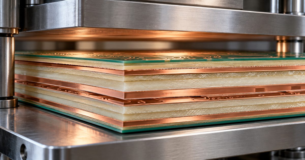
A 0.5 mm PCB can solve a real enclosure or weight constraint, but the thickness should be treated as a controlled mechanical and assembly requirement—not as a simple reduction from a standard board. A thin
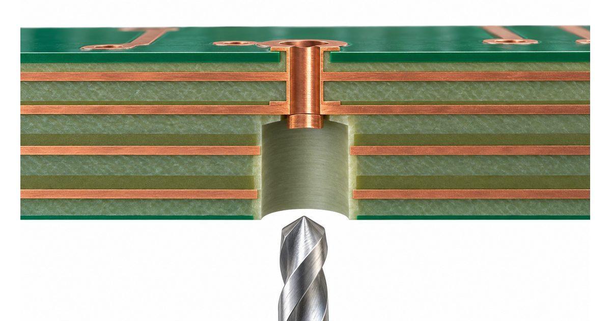
High-speed PCB design begins when a signal's transition time makes the interconnect behave as a transmission line, not when a marketing label reaches a particular clock frequency. The practical task is to preserve a controlled
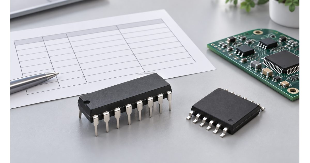
The safest time to qualify an alternate electronic component is before the approved part becomes unavailable. A practical shortage plan separates sourcing evidence from engineering approval: monitor lifecycle notices and supplier risk, define what each
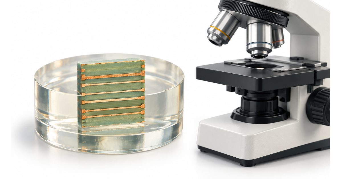
Conductive anodic filament (CAF) testing evaluates the risk of an internal electrochemical migration path forming through a printed board's laminate under temperature, humidity, and electrical bias. The test does not simply ask whether a finished
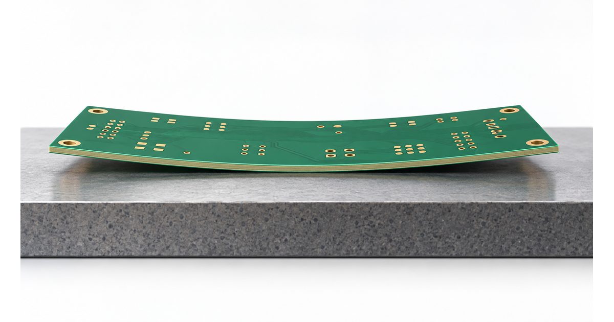
HALT and HASS are related accelerated-stress methods, but they serve different decisions. Highly Accelerated Life Testing (HALT) is a development activity used to expose design weaknesses and explore operating or destruct margins under progressively increased
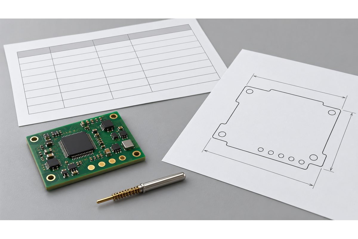
PCB hipot testing applies a specified high voltage across an intended insulation barrier while monitoring current, breakdown, or arcing according to an approved product or safety requirement. It is not a generic “high-voltage board test,”
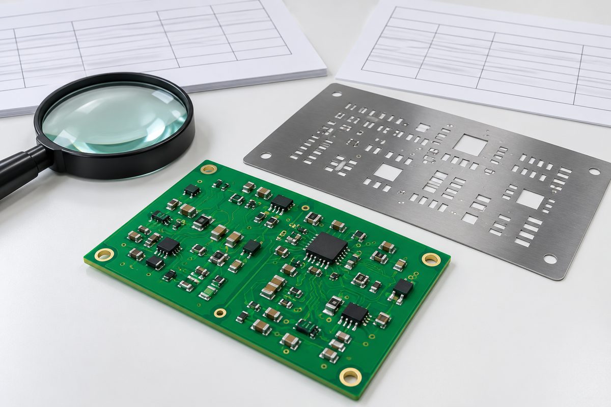
Thermocouple placement for a mixed-thermal-mass PCBA should capture the locations most likely to heat slowly, heat quickly, or approach a component or material limit. Do not spread sensors evenly for appearance or attach them only
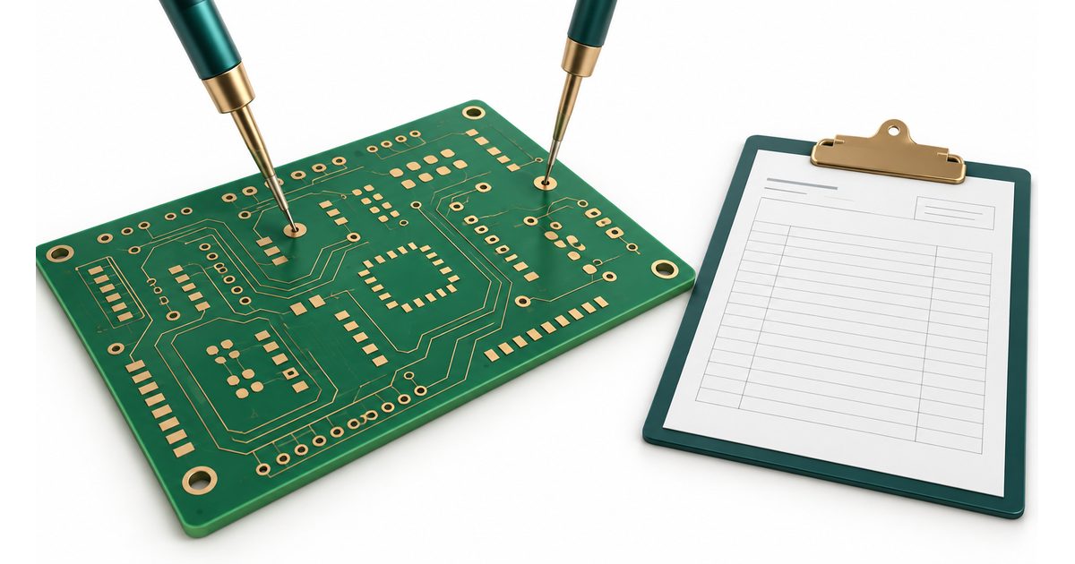
Flying probe and bed-of-nails testing can both check PCB assemblies for electrical manufacturing defects, but they create different cost and schedule profiles. Flying probe uses moving test heads and usually avoids a dedicated contact fixture,
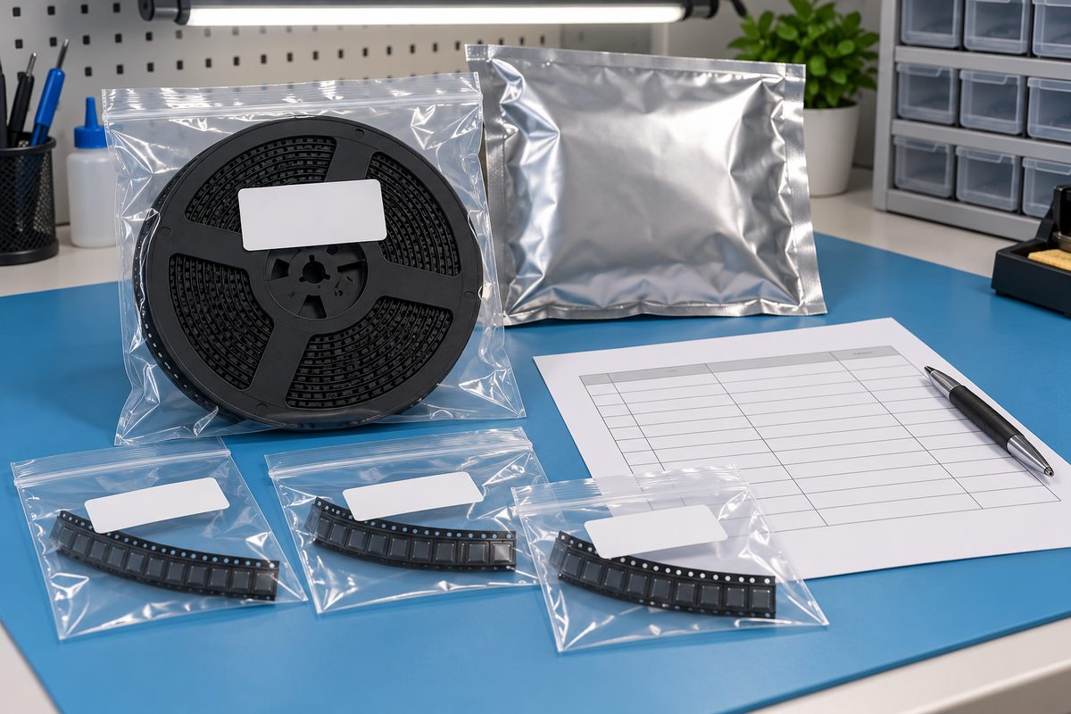
Electronic components incoming quality control (IQC) is a risk-based receiving process that confirms the delivered parts match the approved purchase requirement, retain usable condition, and carry the traceability required for the product. IQC does not
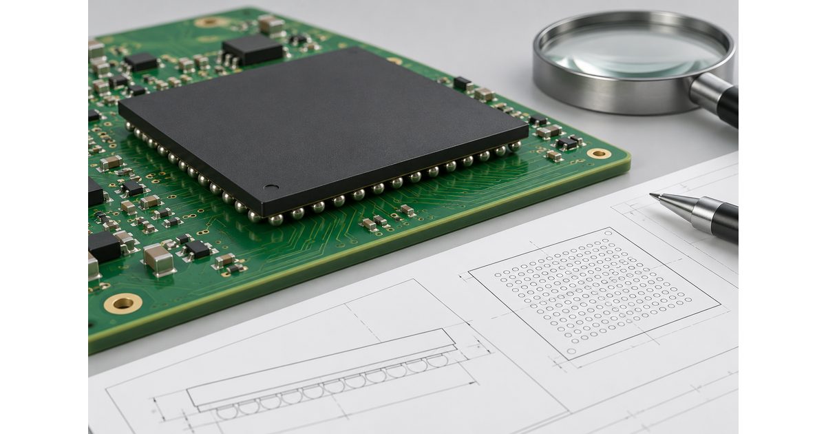
QFN solder voiding is the presence of gas pockets or unfilled areas within the reflowed solder layer, most often beneath the exposed thermal pad. An X-ray image can show their projected location and area, but
Email us for a Free Quote: [email protected]
PCB MANUFACTURING & ASSEMBLY
Start your next PCB project
Share your requirements for PCB fabrication, assembly or component sourcing.

PCB fabrication, assembly and component sourcing — from prototype to production.
Orinew Technology Development Co., LTD.
Contact our team
Address17th Floor, 2B Bldg., Creative Bldg., Time Valley, Heshuikou Community, Matian Street, Guangming Dist., 518106 Shenzhen, China© 2012–2026 Orinew Technology Development Co., LTD.