
AOI, X-Ray and ICT: A QC Plan for Labeling Machine PCBAs

Table of Conent
Table of Conent
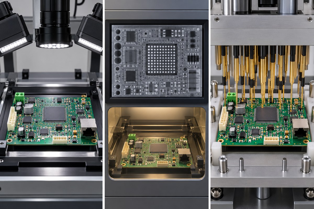
AOI, X-ray inspection, and in-circuit test (ICT) are not interchangeable quality gates for a labeling-machine control board. AOI is strongest at visible placement and solder features, X-ray reveals hidden interconnects and internal solder conditions, and ICT electrically checks accessible nets and components. A reliable QC plan assigns each method to a defined defect mechanism, then closes the remaining risk with programming, functional test, and traceable acceptance data. Using every method on every board is not automatically better; coverage must match the design, production volume, failure consequences, and available test access.
For a servo labeling machine, the PCBA may coordinate sensors, encoder inputs, motor drives, communications, safety interlocks, and print or apply timing. A cosmetic inspection result cannot prove those functions, while a powered functional test may pass even when a marginal solder joint is waiting to fail. The release package therefore needs a layered test strategy rather than one generic note such as “100% tested.”
Begin with a defect-to-test coverage matrix
The best inspection plan starts by listing credible defects and the evidence required to detect them. Component omission, wrong polarity, skew, lifted leads, solder bridges, open joints, BGA voiding, incorrect resistor values, shorts, programming errors, and unstable sensor inputs do not share one universal detection method. The matrix should name the test stage, sampling or 100% rule, acceptance criterion, reaction plan, and record retained for each risk.
IPC announced the 2024 J revisions of J-STD-001 and IPC-A-610 as complementary process and assembly-acceptance documents. The IPC-A-610J table of contents and scope also make an important boundary clear: visual acceptance criteria do not by themselves define X-ray evaluation. Procurement teams should identify the applicable revision, product class, customer deviations, and any design-specific limits instead of treating “IPC compliant” as a complete test specification.
Use AOI for visible placement and solder evidence
AOI is the primary high-speed screen for visible surface defects after solder paste printing, placement, reflow, or selective soldering. According to Nordson’s overview of automated optical inspection systems, typical detectable conditions include missing or misaligned components, polarity errors, solder bridges, lifted leads, and insufficient or excess visible solder. Two-dimensional systems analyze surface contrast and geometry, while three-dimensional systems add height and volume information.
For a labeling-machine controller, AOI should focus on timing-critical sensor interfaces, servo communication circuits, fine-pitch ICs, polarized protection parts, optocouplers, connectors, and any hand-placed component that can be omitted or rotated. The program needs controlled golden data, component libraries, lighting, board support, and revision management. A threshold copied from another assembly can create either escapes or excessive false calls.
AOI cannot see through opaque packages or underneath most BGAs, QFNs, bottom-terminated components, shields, and tall neighboring parts. It also does not prove resistance values, continuity through inaccessible paths, firmware, or real machine timing. Operators must review suspect images under a documented disposition process; an automatically generated pass/fail flag is not a substitute for calibrated criteria and defect feedback.
Add X-ray only where hidden joints justify it
X-ray inspection is valuable when critical solder geometry is hidden from optical view. It can show BGA ball alignment, bridging, missing connections, gross opens, void patterns, and solder distribution under bottom-terminated packages. Nordson’s inline AXI platform description identifies PCB assembly and SMD solder-joint inspection as core applications.
The X-ray plan should identify exactly which packages and defect modes need evaluation. A blanket “X-ray inspected” statement says little without views, magnification, angle, algorithm, sample rule, and acceptance limits. Two-dimensional images can overlap features from both board sides. Computed tomography or angled views may separate structures, but they add cycle time, programming effort, equipment constraints, and interpretation requirements.
Void percentage alone is not a universal reliability verdict. Package type, thermal-pad function, joint geometry, product requirements, and the governing specification determine what matters. X-ray also cannot confirm component value, code execution, analog calibration, or connector pin function. Use it to close hidden-structure risk, not to replace electrical or functional evidence.
Use ICT for structural electrical faults and component values
ICT applies controlled measurements through test probes, boundary scan, or related access methods. Keysight describes in-circuit testing as a manufacturing test capable of detecting conditions such as opens, shorts, irregular resistance, unexpected capacitance, polarity problems, missing parts, and incorrect component values. It can isolate faults at component or net level, which makes repair faster than a final functional failure with no diagnostic location.
Coverage depends on design for test. Test-pad size, spacing, probe access, ground distribution, isolation options, power domains, component topology, and panel support all affect what the fixture can measure. Dense layouts, BGAs, RF networks, parallel components, and protected high-impedance nodes can reduce direct access. Keysight’s manufacturing guidance notes that ICT may need AOI, AXI, boundary scan, or functional test to cover these gaps.
A bed-of-nails fixture adds nonrecurring engineering cost and maintenance, but it can provide repeatable throughput for stable medium- or high-volume products. Low-volume or frequently changing variants may favor flying probe, boundary scan, modular fixtures, or a narrower ICT scope. The decision should compare fixture amortization, diagnostic value, cycle time, test-point impact, variant control, and likely field cost—not only unit test price.
If the design is approaching release, provide the Gerbers, BOM, pick-and-place data, schematic or netlist, variant rules, target volume, and preliminary coverage matrix through our testability and fixture review for the complete assembly package. The review can identify inaccessible nodes, fixture assumptions, inspection limits, and functional-test inputs before tooling is committed.
Place each gate where it can prevent downstream cost
Inspection timing matters as much as technology selection. Solder paste inspection can catch print defects before components consume value. Post-placement checks can detect gross setup errors before reflow. Post-reflow AOI provides immediate process feedback. X-ray should follow the process that creates the hidden joint, while ICT usually follows assembly completion and cleaning when required. Programming and functional test occur after the board is safe to power.
A practical route might be SPI for fine-pitch paste deposits, AOI after reflow, targeted X-ray for BGA/QFN devices, ICT for accessible structural faults, firmware programming with checksum capture, and a final powered test for sensor, communication, and motor-control interfaces. This is a risk-based example, not a universal recipe. Our overview of the PCB assembly process and quality controls explains how inspection gates relate to the wider manufacturing sequence.
Do not confuse inspection with functional proof
A labeling controller must ultimately behave as a system. Functional test should exercise representative supply ranges, digital and analog inputs, encoder or sensor channels, communications, outputs, interlocks, and fault reporting. Motor-power stages may need simulated loads or safe external fixtures rather than direct machine connection. The test specification should define limits, stabilization time, calibration state, firmware version, and pass data.
AOI can confirm that a transceiver appears correctly placed; ICT may verify nearby values and continuity; X-ray may evaluate hidden joints; yet only an appropriate powered test can show whether the communication channel exchanges valid data. Conversely, a short functional cycle may not expose a marginal joint that AOI or X-ray can identify. The methods complement each other because they answer different questions.
The older AssyPCB discussion of manufacturing-test challenges for complex PCBAs is useful background on electrical access and coverage constraints. For controller-level delivery, the same principle extends to enclosure wiring and interfaces; our controller box-build acceptance-test guide shows why harnesses, grounding, I/O, and final configuration need their own evidence.
Control revisions, false calls, and reaction plans
Every inspection program and fixture must be tied to the released PCB, BOM, centroid data, schematic or netlist, firmware, and approved variants. A substituted component can change AOI appearance, X-ray density, ICT limits, or powered behavior without changing the basic reference designator. Revision control should therefore cover inspection libraries, limit sets, fixture wiring, test software, golden samples, and operator instructions.
False calls deserve measured management. If AOI thresholds are loosened merely to improve first-pass statistics, real defects may escape. If thresholds are too tight, inspectors may normalize repeated alarms and miss the important one. Review defect paretos, confirmed-versus-false-call rates, escape data, and program changes. Link each confirmed defect to containment, root-cause analysis, correction, and reinspection of affected work in process.
The assembly drawing is one control point for these requirements. A clear PCB assembly drawing checklist helps keep polarity, special handling, workmanship, coating, marking, and test notes aligned with the actual revision. The test plan should reference controlled documents rather than restating them inconsistently.
Specify the evidence that must ship with the product
A purchase order that says “AOI, X-ray, and ICT required” still leaves major questions unanswered. Define whether testing is 100% or sampled, which packages receive X-ray, what ICT coverage is expected, how false failures are handled, which functional limits apply, and what data must be retained. Also define serial or lot traceability, programming records, fixture verification, calibration status, nonconformance approval, and record-retention expectations.
For prototypes, the most useful deliverables may be annotated defect images, an uncovered-net report, and a list of design changes that improve testability. For production, the priority may shift to stable cycle time, serialized result files, yield trends, and controlled reaction plans. AssyPCB’s PCB assembly service can support a manufacturing route that coordinates sourcing, assembly, inspection, programming, and testing when the released package defines the required evidence and acceptance boundaries.
Build the QC plan around complementary evidence
Use AOI to evaluate visible assembly features, X-ray to investigate selected hidden interconnects, and ICT to locate accessible structural electrical faults. Then use programming and functional test to prove the labeling controller’s required behavior. The correct plan is the smallest defensible combination that covers credible defects, supports diagnosis, and generates records proportionate to product risk.
Before production release, map every critical defect to a test, acceptance rule, reaction plan, and retained record. If you want that matrix reviewed with the manufacturing scope, share the controlled PCB, BOM, test, firmware, and quantity package for engineering evaluation. The resulting scope can separate essential inspection from redundant activity and define what must be verified before the assemblies ship.
Latest Blog





Contact Info
Phone: +86-755-82882936
Email: [email protected]
WhatsApp: +86-13570802455
Wechat: +86-13570802455
Address: 2nd floor,D Bldg.,Electric Link Technology Bldg.,Gongming,Guangming New Dist.,518106 Shenzhen, China