
High-Voltage PCB Spacing: Apply Creepage, Clearance, and Slot Rules
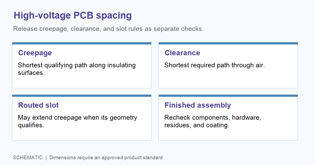
Table of Conent
Table of Conent
High-voltage PCB spacing starts with two separate limits: creepage is the shortest qualifying path along an insulating surface, while clearance is the shortest path through air. A routed slot can increase a surface path when its finished width and geometry qualify under the governing standard, but it does not automatically increase clearance. Select the applicable product safety standard and insulation class first; then determine working voltage, transient exposure, pollution degree, material group, altitude, and finished assembly geometry. A generic voltage-to-millimeter rule cannot replace that sequence.
For a build-ready design, put each barrier’s approved creepage and clearance requirements on a controlled drawing, identify where a slot is credited, and specify how fabrication and assembly will preserve the path. The finished board, not just nominal CAD artwork, is the object to review. This article focuses on the handoff between design, fabrication, component sourcing, assembly, and inspection.
Which requirement sets the spacing?
The end product and its applicable safety requirement set the insulation objective. IEC 60664-1 provides insulation-coordination principles and methods for clearances, creepage, and solid insulation within its stated scope; a product-specific standard may set additional or different conditions. Do not select a number from a general PCB chart before identifying the requirement that governs the finished equipment.
Build a barrier register that identifies the two conductive domains, the insulation function, the working voltage and waveform, expected transients or overvoltage category, pollution degree, material group or verified comparative tracking index (CTI), altitude, and any qualified coating system. Basic, reinforced, and functional insulation are distinct design objectives. The product safety engineer should approve which applies to each path. Texas Instruments’ design guidance likewise separates the inputs for creepage and clearance rather than deriving both from one voltage figure.
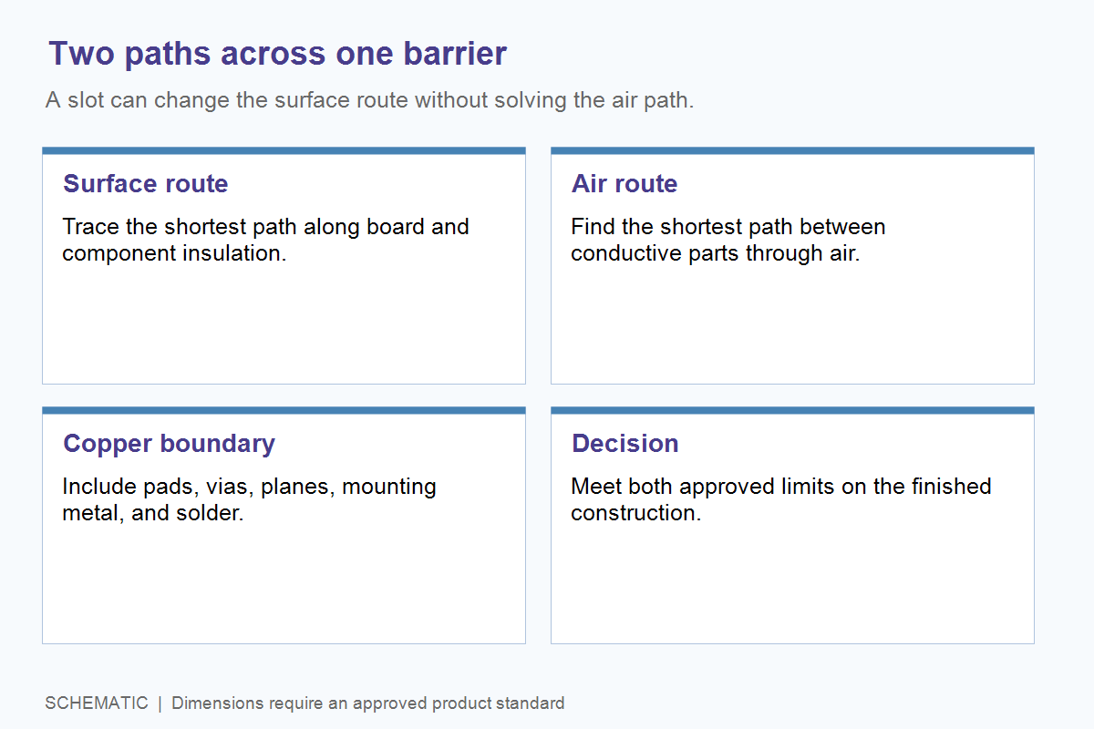
A useful first review asks whether the hazard boundary in the schematic matches the physical boundary on every layer. A copper pour, plated hole, mounting screw, connector shield, component lead, or heat sink can make a shorter path than the two traces the layout designer originally measured. The PCB hipot test planning guide explains why a test path must be mapped across the actual assembly; a spacing check needs the same discipline before test planning begins.
When does a routed slot help?
A qualifying routed slot may lengthen creepage by forcing the surface route around or through the cutout. It does not fix an inadequate direct air gap. Its credited contribution depends on the relevant standard, pollution degree, finished slot width, depth or through-cut geometry, and the shortest remaining path. TI’s power-supply design seminar explicitly notes that a slot may improve creepage while having no effect on clearance. The example width table in that publication is tied to its cited IEC method; it is not a universal fab allowance.
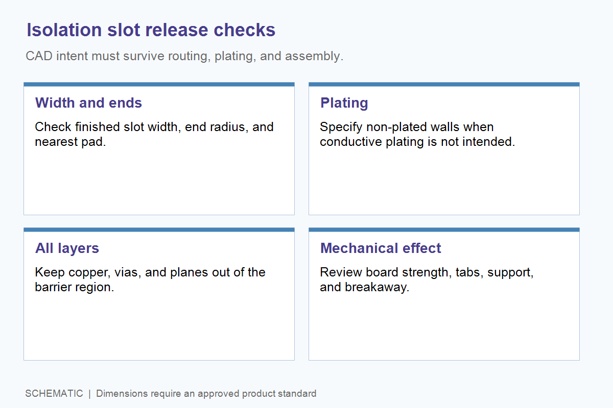
Before deciding that a slot saves board area, check four things. First, trace the surface path around both slot ends, not only across its middle. Second, measure the air path between the nearest exposed conductors, component pins, and hardware. Third, confirm the fabricator’s finished routing capability, end radius, location tolerance, and whether the feature is non-plated. Fourth, confirm that the remaining board web and assembly support are mechanically adequate. A narrow, plated, blocked, or misplaced cutout may not provide the insulation path assumed in CAD.
The PCB slot release guide covers plated versus non-plated definition and routing output. For an insulation slot, the manufacturing drawing should identify the barrier purpose as well as the finished dimension and plating intent. If the existing footprint cannot fit both approved spacing limits, share the barrier map, layout, and proposed slot geometry for a fabrication and assembly review before freezing the outline. Include the governing standard and the allowed design changes so the response addresses the actual safety constraint.
How do you check the finished assembly?
Assess spacing after component placement, soldering, cleaning, coating, and integration, because each stage can alter the shortest path. Solder fillets, residues, displaced wires, component bodies, adhesive, coating edges, mounting hardware, and enclosure surfaces deserve a path-by-path review. A bare-board rule check is necessary, but it is not evidence that every populated assembly path remains compliant.
Do not treat solder mask or an unspecified conformal coating as an automatic spacing exemption. Credit a coating only when the applicable standard permits it and the material, thickness, coverage, cleaning, cure, inspection, and maintenance conditions are qualified. Similarly, laminate CTI is a material property relevant to creepage evaluation; a generic FR-4 label is not evidence of a particular material group. The PCB lamination guide shows why a named material and controlled stackup are more useful than a generic construction label.
For multilayer boards, inspect copper on all layers around the intended boundary and note the required dielectric construction separately. A slot may remove material needed for rigidity or expose an edge to contamination. If an insulating component bridges the boundary, review its package creepage, clearance, rated working voltage, and mounted footprint together. The component’s isolation rating does not waive an inadequate board layout.
What should the PCB fabrication package specify?
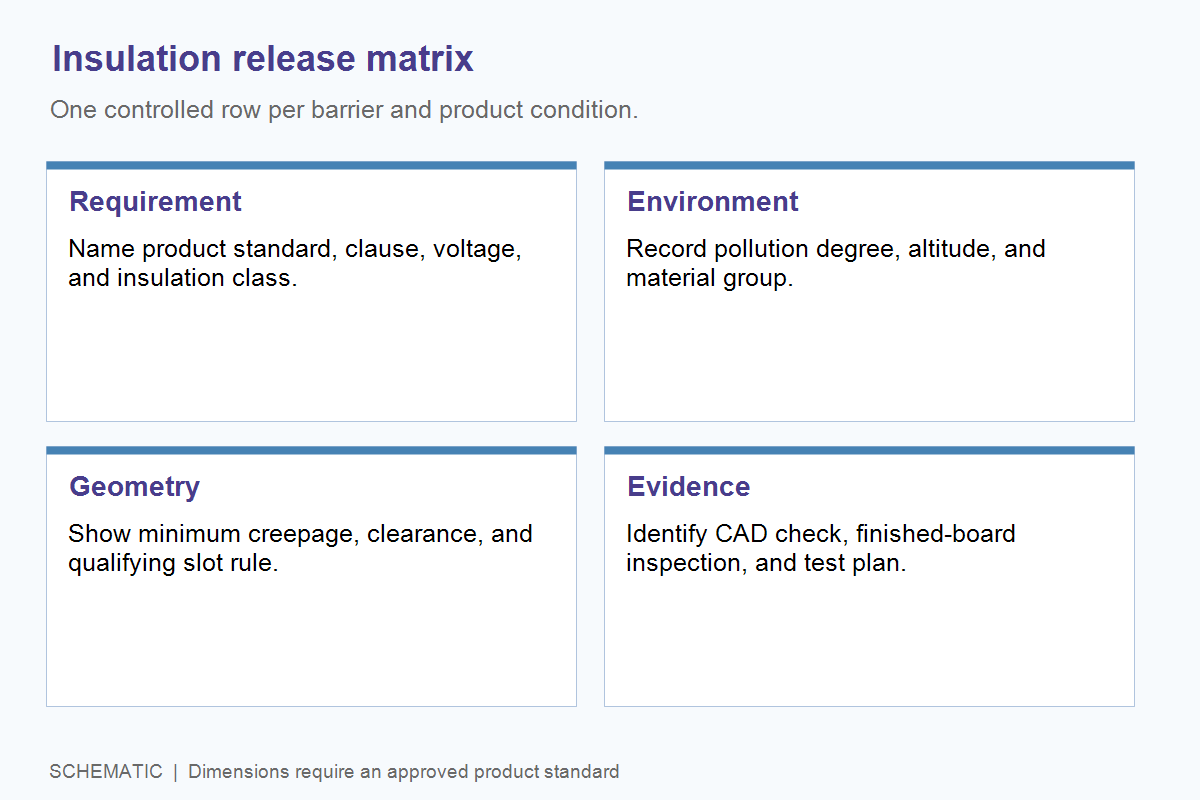
The supplier should receive an insulation schedule that can be checked without inferring safety intent from Gerbers. Tie each barrier to a controlled net pair, approved requirement and revision, minimum finished geometry, material condition, slot rule if used, and inspection or test evidence. The matrix below is a release template; values must be filled from the applicable product requirement, not from this article.
| Release item | What to provide | Decision it supports |
|---|---|---|
| Safety basis | Product standard and clause, insulation class, named domains | Which barrier and rule set apply? |
| Electrical condition | Working voltage and waveform, transient condition, overvoltage category where applicable | Which creepage and clearance derivations are required? |
| Environment and material | Pollution degree, maximum altitude, qualified laminate CTI/material group, qualified coating if credited | Are the assumed insulation conditions valid? |
| Finished geometry | Approved minimum paths, measurement endpoints, slot finished width and location, plating intent, all-layer keepout | Can fabrication preserve the credited path? |
| Acceptance evidence | CAD rule check, first article measurement, visual inspection, and separately approved electrical test plan | What proves the released construction was built? |
Specify whether a value is nominal or minimum after manufacturing tolerance. The drawing should call out the approved measurement endpoints and what happens if CAM asks to move copper or alter a slot. An unapproved modification can shorten the critical path even if it appears manufacturable. The full turnkey PCB assembly service is relevant when the same release needs fabrication, sourced isolation components, assembly, and test scope coordinated in one quotation.
Which checks are design evidence, and which are tests?
Keep geometric verification and dielectric testing separate. A CAD and finished-board inspection can show that the specified paths and materials were built; a defined hipot test challenges a particular insulation barrier under a specified electrical condition. A passed test does not establish that an undersized creepage path will resist long-term tracking in the intended environment. Conversely, a measured distance alone does not prove that the finished assembly withstands its required electrical stress.
Ask the safety owner whether the applicable requirement calls for design qualification, production testing, sampling, or finished-product testing. Record the test nodes, voltage type and level, ramp, dwell, trip criteria, discharge, and product configuration separately from the dimensional release. The PCB test planning framework helps link a failure mode to a method and acceptance record. If a high-voltage test is specified, its setup must be approved by qualified personnel; do not substitute a generic test recipe.
What changes cost or lead time in an RFQ?
Pricing and schedule depend on which condition drives the build. A wider board to preserve both paths changes material usage and panelization; a routed slot adds geometry, programming, inspection, and potentially handling constraints; a specified high-CTI laminate or qualified coating can affect sourcing and process control. A custom first-article measurement or defined electrical safety test adds scope. None of these choices is automatically cheapest: compare them against the same approved insulation requirement and finished assembly drawing.
Release Gerbers or ODB++, the stackup, schematic barrier map, BOM with isolation component part numbers, placement data, fabrication and assembly drawings, quantities, and the approved acceptance matrix. State which substitutions need safety approval. If a supplier proposes a different laminate, isolator package, coating, slot width, or board outline, require the product owner to recheck both creepage and clearance before acceptance. A small purchasing substitution can invalidate the original path even when electrical function is unchanged.
The practical sequence is to approve the rule set, map each physical barrier, verify the shortest surface and air paths, and then release finished geometry and evidence requirements. For a project that needs fabrication, component sourcing, assembly, and defined insulation testing together, share the controlled build package and barrier schedule so the engineering review can scope the construction and quotation against the same safety assumptions.
Technical references
IEC 60664-1, insulation coordination overview (edition information visible on IEC site, accessed October 20, 2026); Texas Instruments, Demystifying Clearance and Creepage Distance for High-Voltage End Equipment (March 2024, accessed October 20, 2026). Use the applicable full standard and product safety review for the project-specific limits.
Latest Blog





Contact Info
Phone: +86-755-82882936
Email: [email protected]
WhatsApp: +86-13570802455
Wechat: +86-13570802455
Address: 2nd floor,D Bldg.,Electric Link Technology Bldg.,Gongming,Guangming New Dist.,518106 Shenzhen, China