
Copper-Core PCB Stackup: Specify Dielectric, Mounting, and Inspection
Table of Conent
Table of Conent
A copper-core PCB is useful only when the complete heat path, electrical isolation, and mounting interface are defined together. The copper base can spread heat, but it does not remove the thermal resistance of the dielectric, an imperfect board-to-heatsink contact, or a poorly specified fastener. Before releasing an insulated metal substrate (IMS) design, identify the exact copper circuit, dielectric, and metal-base construction; state whether the base is electrically floating, grounded, or connected by an approved feature; and define how the finished assembly will be inspected. If those conditions are unknown, compare a copper-base proposal with aluminum IMS and a conventional board using the same thermal and electrical acceptance limits.
Decide whether the copper base solves the measured thermal problem
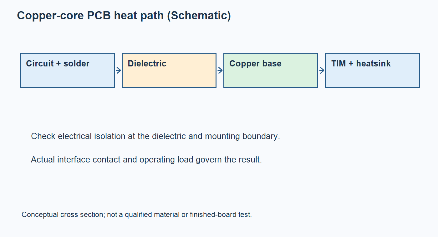
The decision starts at the component junction, not at a metal conductivity value. List each significant heat source, its operating loss, duty cycle, ambient range, and permissible junction or case temperature. Draw the route from package pad through solder, circuit copper, dielectric, base metal, interface material, heatsink, and ambient. A material change only helps if it lowers enough resistance in the limiting part of that chain.
Henkel’s THERMAL CLAD selection guide describes an insulated metal board as a copper circuit, dielectric, and metal base, and notes that aluminum is common while copper is an available base option. That is a construction description, not proof that every copper-base design meets a target temperature. Texas Instruments’ FR-4 versus IMS thermal comparison shows that interface contact and clamping can materially change the result even when the board construction is known. Its tested geometry and interface materials are examples, not universal copper-core performance figures.
Compare candidate stacks using the selected device losses and the same enclosure, heatsink, airflow, and measurement locations. If heat is concentrated under a small device, ask whether dielectric thickness and thermal impedance dominate before paying for a heavier base. If the bottleneck is the board-to-heatsink interface, improve flatness, contact area, fastener placement, or the specified thermal interface material first. A copper plate that stops at a poor contact joint is an expensive heat spreader with no verified system benefit.
Release the dielectric as an electrical and thermal part
The dielectric is the controlled barrier between the circuit and the metal base. Its material designation, finished thickness, thermal impedance or conductivity, voltage withstand requirement, and operating-temperature qualification should be explicit in the fabrication drawing. Ask the fabricator which values describe the material sheet and which will be verified on the finished board. Do not turn a published typical value into an incoming acceptance limit without agreement.
For a first-pass thermal comparison, a uniform dielectric’s area-normalized resistance is approximately thickness divided by thermal conductivity. This screening relation assumes one-dimensional flow and does not capture spreading, solder voids, edge effects, or interface contact. Reducing dielectric thickness may lower thermal resistance but can conflict with the electrical isolation margin or process variation. The supplier’s specific material data and the product’s voltage requirement must govern that tradeoff. Henkel’s guide lists different dielectric constructions and illustrates that thermal and electrical properties vary by family.
State whether the base is an electrical reference, a protective-earth path, or intentionally isolated from circuit nodes. Then mark mounting holes, exposed edges, chassis contact points, connectors, and any proposed pedestal or direct thermal path on the drawing. A generic plated via cannot simply be assumed to pass through an insulated metal base: its geometry and isolation must be engineered and approved for the chosen construction. Where a direct metal-to-device contact is proposed, verify the device pad’s electrical potential before treating it as a thermal shortcut.
Use mounting and machining notes to protect the intended interface
The mechanical drawing must tell the fabricator and assembler which surfaces establish thermal contact. Dimension the metal-base thickness, finished board outline, hole positions, counterbores or slots if applicable, and the intended contact land. Identify any regions that must stay flat, free of burrs, free of coating, or protected from unintended chassis contact. Avoid calling a generic PCB thickness without stating where it is measured; the finished-thickness and fit guide explains why the measurement basis and mating hardware need to agree.
Specify the thermal interface material (TIM) as part of the assembly, including its approved product or performance envelope, application area, and clamp or fastening method. Do not assume that a thin high-conductivity TIM will outperform another product when contact pressure is inadequate. In the TI comparison, a different interface approach was selected for the FR-4 sample because its mounting geometry did not maintain the same contact as the IMS sample. That observation supports testing the actual hardware, not copying its material dimensions or temperatures into a new specification.
If the drawing calls for a hole that crosses or approaches the dielectric boundary, ask the board supplier to show the intended section before routing. Document whether an exposed copper edge is acceptable, whether a fastener may connect the base to chassis, and what isolation test applies after machining. Treat these as product-specific questions because the safe answer depends on the voltage architecture and enclosure. A revised hole or hardware choice can change both thermal contact and electrical isolation.
At this stage an engineer can resolve major cost drivers before fabrication files are frozen. If the dielectric choice or mounting geometry is still open, share the proposed stack and heatsink drawing for review with device losses, voltage boundary, expected quantity, and the intended contact method. Ask for a buildability and assembly-scope assessment before deciding that a copper base is required.
Check the fabrication and assembly sequence as one build
A manufacturable copper-core drawing needs more than a layer count. Identify the circuit foil, dielectric code and thickness, copper-base material and finished thickness, surface finish, solder mask, outline, and critical hole details. Agree which tolerances are necessary for fit or thermal contact and which are supplier process choices. IPC’s IPC-6012F scope and contents explicitly include metal-core printed boards; cite the applicable purchase specification and acceptance class rather than inventing a special copper-core quality label.
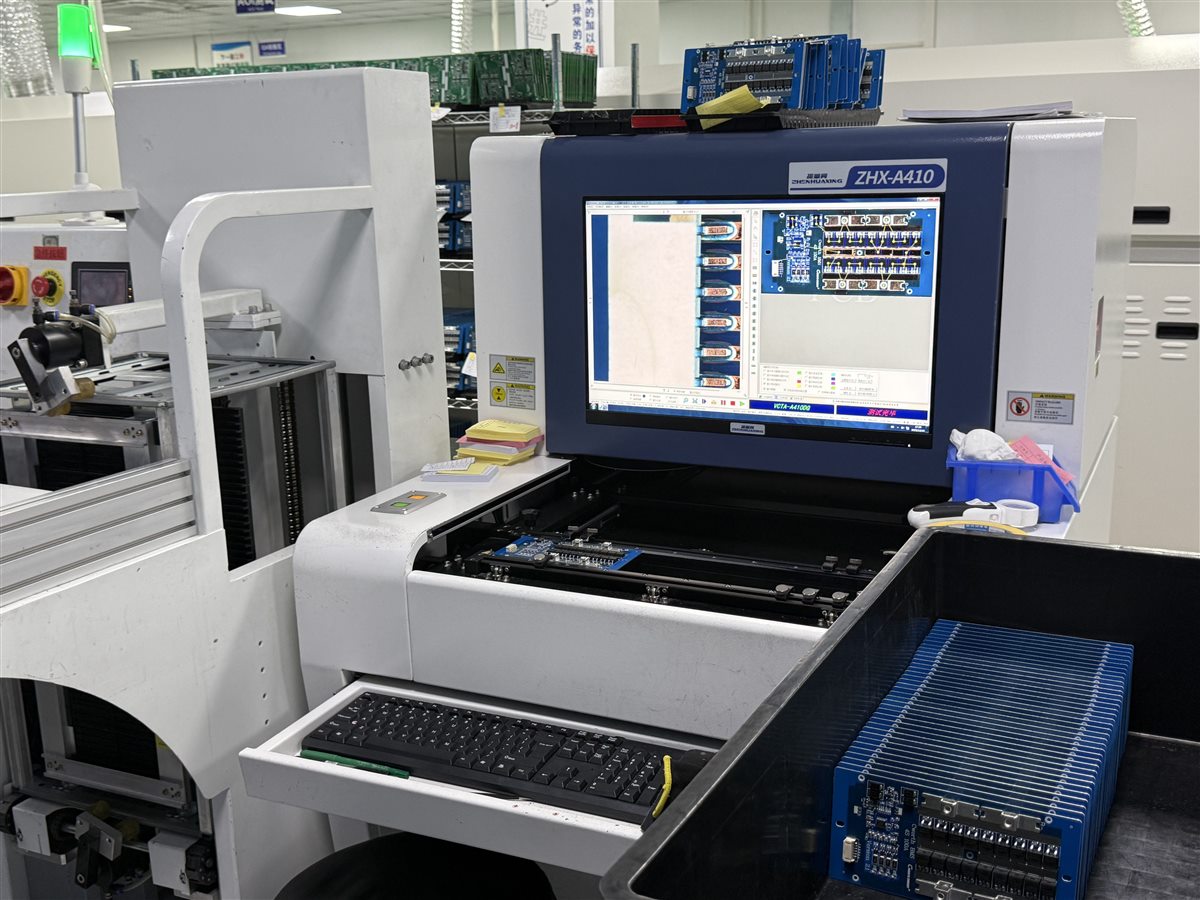
Assembly planning follows the same thermal path. Check the component package pad, stencil aperture, reflow support, inspection view, connector orientation, and the operation that attaches the board to the heatsink. An AOI program can inspect visible placement and solder features, but it cannot by itself demonstrate dielectric isolation or the final thermal interface. The assembly drawing checklist helps keep population, polarity, hardware, and variant details aligned with the released BOM and placement file.
Plan panelization and handling around the finished metal-base geometry. A board with tight contact-land requirements may need support, edge protection, and a controlled depaneling approach. Explain who supplies the TIM and fasteners and who performs the heatsink attachment. If the quoted scope ends at a bare board, do not assume the assembler has verified the mounting surface or contact pressure. The PCB DFM report guide is useful for separating release-blocking construction conflicts from alternative material or tooling suggestions.
Choose inspection evidence that answers the actual failure risk
Choose inspection and test evidence from the risk, not from a generic certificate list. The buyer needs to know which requirement is checked on the laminate or bare board, which is checked after assembly, and which requires the final heatsink and enclosure. A visual bare-board inspection cannot prove that the powered device stays within its temperature limit; an operating temperature test cannot replace a required isolation check.
| Risk or decision | Release input | Evidence to request | Action if unresolved |
|---|---|---|---|
| Dielectric thermal bottleneck | Selected material, finished thickness, heat load, contact area | Material data and an assembly-level temperature measurement at the stated operating condition | Compare stack and heatsink alternatives against the same limit |
| Unintended circuit-to-base contact | Voltage boundary, mounting holes, edge treatment, grounding intent | Agreed electrical isolation test and inspection locations | Revise the section, hole, or hardware before release |
| Poor heatsink contact | Contact land, flatness need, TIM, fastener pattern | Fit and interface inspection plus operating temperature result | Correct geometry or clamping before changing base metal |
| Unclear supply scope | Fabrication data, BOM, placement, hardware, test limits, quantity | Supplier-specific DFM findings and quoted test ownership | Normalize RFQs before comparing price |
Record the measurement condition for each result: device load, ambient, airflow, heatsink configuration, and board revision. A temperature reading without those conditions is difficult to compare with simulation or a second supplier’s sample. Where the metal base is electrically accessible, define the dielectric test method and limits through the applicable product safety and procurement requirements rather than selecting a generic withstand voltage from an unrelated material brochure.
Keep the evidence linked to the released revision. A material substitution can alter dielectric thermal impedance, breakdown behavior, base thickness, machining, and assembly support. Treat it as a controlled engineering change, even if a substitute’s catalog thermal conductivity appears similar. Procurement should ask which characteristics are fixed, which substitutions need approval, and which inspection records will accompany a repeat build.
Compare total build scope, then release one controlled package
Copper-core PCB cost should be compared at the assembled-product level. A lower bare-board price can be offset by extra machining, difficult handling, interface hardware, manual assembly, inspection, or a fixture change. Conversely, a more expensive substrate may simplify the enclosure only when that effect is demonstrated in the actual product. Ask each supplier to quote the same material, board revision, quantities, finish, test limits, TIM and heatsink responsibility, and approved alternatives. The full turnkey assembly scope provides a starting point for coordinating fabrication, parts, assembly, and testing; confirm the specific metal-core construction and responsibilities in the RFQ rather than assuming they are standard capabilities.
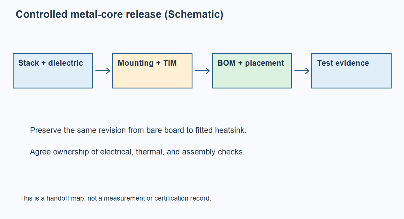
Release Gerber or another agreed fabrication dataset, drill and route files, a dimensioned stack and mechanical drawing, BOM, placement file, assembly views, approved material alternatives, quantities, and a test plan. Identify the thermal measurement locations and the electrical isolation boundary. Keep the copper-base and heatsink revisions aligned. The most useful deliverable is a short list of open DFM questions with owners and due decisions, not an unsupported promise that any particular metal will run cooler.
A copper core earns its place when the verified assembly meets the thermal limit while preserving insulation, fit, and an inspectable production path. Once the package is controlled, send the fabrication and assembly files for a scoped evaluation with the dielectric specification, heatsink and TIM details, build quantity, and acceptance tests. The review can then clarify feasibility, sourcing, test ownership, and comparable quotation assumptions.
Latest Blog
Contact Info
Phone: +86-755-82882936
Email: [email protected]
WhatsApp: +86-13570802455
Wechat: +86-13570802455
Address: 2nd floor,D Bldg.,Electric Link Technology Bldg.,Gongming,Guangming New Dist.,518106 Shenzhen, China