
Smart Grid PCB Design: Release Metering, Relay, and EMC Evidence
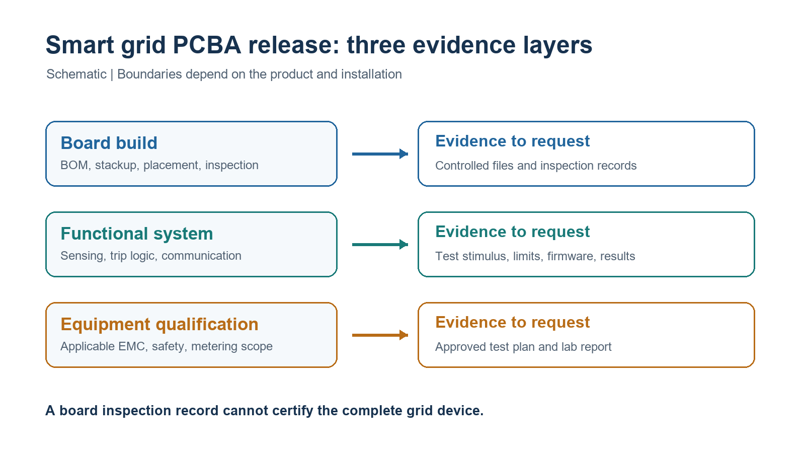
Table of Conent
Table of Conent
Smart grid PCB design starts by naming the equipment, its external ports, and the evidence each board can actually provide. A protection relay, a transformer-operated revenue meter, and an IEC 61850 communication IED may share sensing and Ethernet parts, but they do not share one automatic compliance checklist. The product owner should assign the applicable standards and test levels; the PCBA release should then preserve the specified isolation geometry, assembly configuration, measurement access, and revision identity. Board inspection can establish that a controlled assembly was built. Calibrated metering, protection behavior, network interoperability, and equipment immunity need their own system or laboratory evidence. This separation prevents a good-looking PCB from being mistaken for a qualified grid device.
Start with the equipment role before choosing a standard
IEC 61850 addresses information models and communication in power utility automation; it is not a substitute for a metering accuracy or EMC test plan. The IEC 61850 project explains that the series extends beyond a single wire protocol. For substation communication and automation IEDs, IEC 61850-3:2013 describes general construction, design, and environmental requirements. The product specification must state which parts apply to the particular device and installation.
A protection relay has a different equipment scope: IEC 60255-26:2023 specifies EMC requirements for measuring relays and protection equipment, including related control, monitoring, communication, and process interface equipment. By contrast, IEC 62053-22:2020 applies to type testing specified classes of transformer-operated static AC active-energy meters. A relay board does not gain a meter class because it contains an ADC, and a PCB supplier cannot certify either finished product by providing an assembly inspection record.
| Product role | Requirement to assign | Useful PCBA release evidence | Evidence outside board inspection |
|---|---|---|---|
| Utility communication IED | Relevant IEC 61850 functions, configuration, interface, and environmental scope | Ethernet and power BOM, interface pinout, firmware identity, assembled-board electrical checks | Interoperability and installed-system behavior against the approved configuration |
| Protection relay or process interface | Product-owner-selected IEC 60255-26 EMC plan and protection function requirements | Port protection BOM, spacing drawing, inspection and functional fixture records | Qualified equipment-level disturbance and trip-performance results |
| Transformer-operated energy meter | Applicable metering class and test scope, such as IEC 62053-22 where relevant | Sensor and analog-front-end revision, calibration access, assembly traceability | Type-test accuracy across specified conditions and approved calibration procedure |
This is a responsibility map, not a claim that every grid assembly needs all three standards. Record the actual device role, market, voltage and installation conditions before choosing a PCB stackup or test fixture.
Keep sensing, trip, and communication boundaries explicit
A shared PCB can carry several functions, but each function needs its own failure observation. For metering, document the current sensor, voltage sense path, reference, ADC, calibration constants, and the effect of permitted component substitutions. Texas Instruments compares CT, shunt, and Rogowski sensing and shows why sensor choice changes isolation and the surrounding circuitry. Select the topology from the actual equipment architecture; do not transfer a reference design’s accuracy class to a new assembly without its calibration and type-test evidence.
For a relay output, identify the trip contact or driver, auxiliary supply, fault indication, and reset behavior. For an IEC 61850 interface, record the physical Ethernet port, magnetics or isolation choice, time or configuration dependencies, and the firmware or configuration revision used for validation. These are different acceptance questions. A passing continuity test cannot show that a relay trips under the specified condition, and a successful Ethernet link does not establish application-level interoperability.
The layout drawing should mark sensor, relay, communication, auxiliary-power, and chassis interfaces with their intended return and isolation boundaries. The high-voltage PCB spacing guide is useful when translating the approved insulation design into creepage, clearance, slot, material, and inspection requirements. The equipment owner must supply the working voltage, transient category, environment, and applicable safety interpretation; a generic distance copied from another board is not a release criterion.
If this boundary map is ready for manufacturing review, share the controlled stackup, BOM, connector map, and proposed inspection boundary so fabrication, sourcing, assembly, and fixture assumptions can be checked together.
Trace disturbance paths by port and monitor the function
Surge and fast transients enter through particular ports and return through a particular chassis or ground path. A useful EMC review names the port, applied disturbance, coupling path, monitored function, and pass rule. The laboratory selects the applicable standard edition, waveform, level, and setup with the product owner. The PCBA team supplies the controlled design and accessible observations; it does not infer a universal surge voltage from an unrelated reference board.
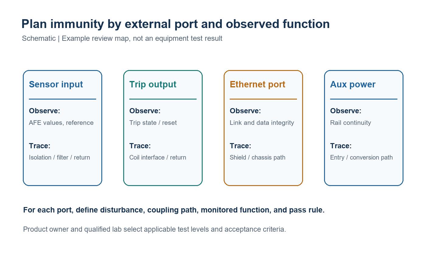
Analog Devices’ AD7606B power-automation application note is a concrete example of this method. Its test board monitors converter timing, status, internal references, and resets while applying ESD, burst, and surge stimuli. The note also explains that a split analog/digital ground joined through a narrow path can concentrate common-mode current during a disturbance. That is a warning to trace return current in the actual assembly, not a universal instruction to join or split every ground plane the same way.
Review the sensing error during and after a transient, not only whether the board stays powered. On a relay, also record output state, unintended trip, and recovery. On a communication IED, record link and application behavior under the approved test conditions. A schematic can anticipate these paths, but only a defined fixture and equipment test can produce the result.
Turn layout choices into build and inspection instructions
The manufacturing package should make the approved electrical boundaries visible to fabrication and assembly. Freeze the stackup, material callouts, finished copper, isolation slots, keepouts, test points, and the mechanical relationship between connectors and chassis. If coating is part of the design, identify coated and uncoated areas plus how coverage will be inspected. The PCBA coating specification guide helps separate an exposure requirement from a process instruction; coating alone does not prove that the complete equipment meets an insulation or EMC requirement.
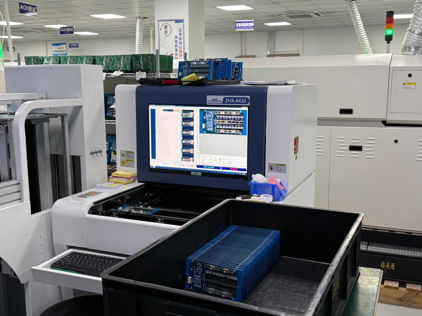
Define inspection by the failure it can reveal. Automated optical inspection can flag visible placement and solder anomalies; it cannot measure meter accuracy or prove a protection algorithm. Hidden joints or high-risk connections may need another agreed inspection method. The AOI, X-ray, and ICT planning example shows how distinct methods answer different assembly questions. Its machine application is different, so use its method-selection logic rather than importing its test limits into a grid device.
Test access should be designed before the board is quoted. Place measurement and programming points where the fixture can reach them without defeating barriers or changing a sensitive analog path. The PCB test-point design guide provides a starting checklist for probe access and release data.
Separate factory screening from equipment qualification
A production matrix should say what is checked on each board, what is checked on a calibrated sample or system, and what belongs to a qualified laboratory. Keep the stimulus, limit owner, fixture, firmware identity, record, and disposition for each row. The example below intentionally has no numeric pass limits: those come from the approved equipment specification and applicable standard edition.
| Question | Board or lot screen | System or lab evidence | Release control |
|---|---|---|---|
| Was the specified assembly built? | BOM/revision check, AOI and agreed hidden-joint inspection | Not a substitute for functional qualification | Record serial or lot, approved substitutions, inspection disposition |
| Is the sensing chain alive? | Safe fixture stimulus and channel/rail readback | Calibrated accuracy over the required range and conditions | Retain sensor, reference, gain, and calibration versions |
| Does the trip or communication path respond? | Defined output and link checks with approved firmware | Protection sequence and IEC 61850 interoperability where required | Record firmware, configuration, timing, and test fixture revision |
| Does the equipment tolerate disturbance? | Continuity and inspection of protection components | Applicable equipment-level EMC setup and monitored behavior | Link the lab report to exact hardware and software revisions |
This split helps procurement ask for evidence that a supplier can actually provide. If the buyer requests a meter class or relay EMC compliance statement, specify whether the purchase covers only PCBA manufacturing, a board-level functional screen, or finished-equipment qualification. Otherwise, the quote can appear complete while the most important acceptance work remains unowned.
Release one configuration and define retest triggers
The final handoff should identify the fabrication outputs, assembly drawing, placement data, approved BOM and alternates, firmware/configuration checksum or identifier, coating and inspection instructions, test fixture revision, and the owner of each acceptance limit. Link every test report to that same controlled configuration. If a sensor, isolator, connector, protection component, substrate, or firmware revision changes, review its affected functions before approving substitution. A purchasing equivalent is not automatically a metrology or immunity equivalent.
For a complete build, the full-turnkey PCB assembly scope connects fabrication and parts sourcing with assembly planning. The buyer still defines the equipment qualification boundary and any independent laboratory work. After the technical release package is complete, teams can provide the fabrication data, BOM, quantities, and board-level test requirements for a joined manufacturing review; the response should clarify sourcing, build, fixture, and inspection assumptions before price or schedule is treated as final.
Final release decision
Release the PCBA when the design files, supplied parts, assembly, and agreed board checks describe one reproducible configuration. Keep metering accuracy, protection behavior, IEC 61850 interoperability, and EMC qualification tied to the approved equipment and test plan. That boundary gives engineering and purchasing a clearer handoff than a single broad claim that a smart-grid PCB is “compliant.”
Latest Blog

Contact Info
Phone: +86-755-82882936
Email: [email protected]
WhatsApp: +86-13570802455
Wechat: +86-13570802455
Address: 2nd floor,D Bldg.,Electric Link Technology Bldg.,Gongming,Guangming New Dist.,518106 Shenzhen, China