
SiC vs. GaN Power Devices: PCB and Assembly Decisions
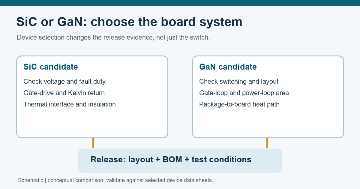
Table of Conent
Table of Conent
Choose a SiC or GaN power device from the converter’s voltage, current, switching, fault, and thermal requirements, then prove that the chosen package can be driven, cooled, assembled, and tested on the actual PCB. SiC often suits higher voltage and current duties; GaN often helps when switching loss and compact magnetics matter. Neither material guarantees a smaller or cheaper finished assembly. A fast device can expose a weak gate return or commutation loop, while a cooler data-sheet number may not describe the board’s actual heat path. Compare candidate part numbers at the intended operating point, then carry the approved footprint, drive circuit, thermal interface, and verification limits into the manufacturing release.
Start with the converter duty, not a material ranking
The first useful comparison is between complete candidate designs under the same electrical and cooling conditions. A generic “SiC is for voltage; GaN is for speed” rule is a screening aid, not a substitute for the selected device’s data sheet. Voltage rating must include the intended bus, credible transients, and the product’s protection strategy. Current and loss estimates must cover the actual waveform, switching frequency, dead time, and ambient conditions.
Texas Instruments describes overlapping end equipment but different voltage, power, and switching strengths for these technologies in its GaN versus SiC review. Infineon likewise notes that a high-frequency GaN advantage depends on topology and board layout in its GaN FET explanation. These are technology-level observations; individual devices and packages can depart from a simple category rule.
| Decision input | SiC candidate: ask | GaN candidate: ask | Evidence to retain |
|---|---|---|---|
| Electrical duty | Does the selected rating and fault strategy cover the real bus and transient case? | Does the selected rating and transient behavior cover the same case? | Part-number data sheet, bus and surge assumptions, protection schematic |
| Loss and frequency | What are conduction, switching, and reverse-conduction losses at the actual operating point? | Do higher frequency and lower switching loss offset any drive, EMI, or thermal penalty? | Comparable loss model and measured waveform at representative load |
| Thermal path | Can the package, interface, PCB, and heat sink reject the predicted loss? | Can the compact package and board copper reject its predicted loss? | Package thermal model, stackup, interface definition, temperature test |
| Board release | Are gate supply, Kelvin return, insulation, and fault sensing defined? | Are drive window, loop geometry, switch node, and assembly process defined? | Controlled schematic, layout, BOM, fabrication and test revisions |
This table is a decision record, not a claim that every SiC or GaN part has the same rating or gate requirements. The selected manufacturer data sheet and reference design set device-specific limits.
Compare the gate and power loops on the same board drawing
Both technologies can switch fast enough for parasitic inductance and coupling to matter. Review the path from driver output through the gate and back to the driver’s return, separately from the high-current commutation path through the switch and local DC-link capacitor. The shortest visible gate trace is not necessarily a short loop if its return takes a detour or shares current with the power source.
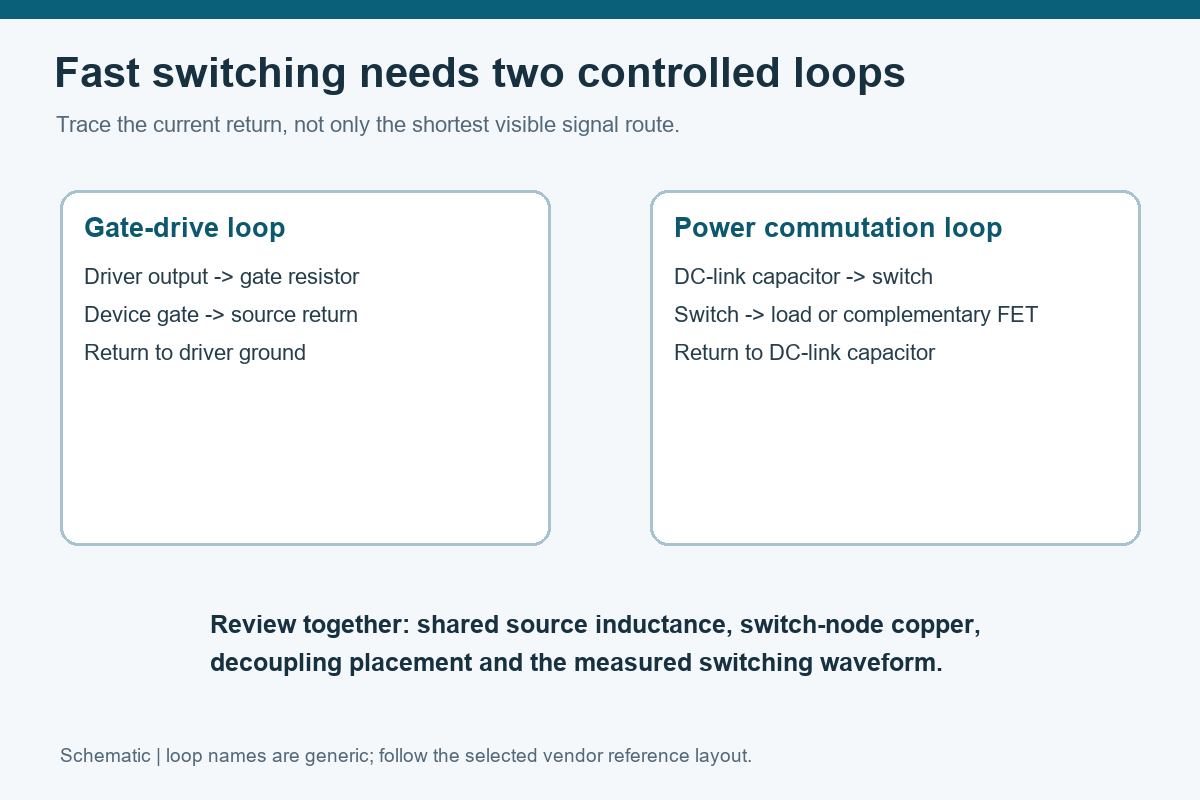
TI’s GaN driver layout recommendations call for a small, controlled gate-drive loop and a short connection between driver ground and FET source. For a SiC package, the same review must account for the actual Kelvin-source option, gate resistance, driver supply and fault sensing specified by its vendor. The practical inspection question is whether the released copper geometry matches the circuit that was characterized, not whether a device label appears on the BOM.
Record the driver part, positive and negative gate limits where applicable, local decoupling, gate resistor values, and any separate turn-on/turn-off paths. Document the switch-node copper and the signal paths most likely to pick up noise. A change from a leaded SiC package to a surface-mount GaN package, for example, can alter the heat path, land pattern, inspection access and assembly sequence. It is a design revision, not a drop-in purchasing substitution.
For high-voltage boards, review the actual working voltage and insulation environment alongside creepage, clearance, and slot decisions. Package voltage rating alone cannot establish PCB spacing. The product safety plan and applicable standard determine the required geometry.
If a different package changes loop placement or insulation geometry, share the proposed stackup and device packages with the heat path and operating conditions. A fabrication and assembly review can scope board construction and access before the layout is released.
Turn the thermal claim into a board-level test
A device’s material thermal property does not specify junction temperature in the finished assembly. Heat crosses die attach, package, solder joint or interface, copper, board dielectric, and sometimes a heat sink or enclosure. Compare the complete thermal path for each candidate package under the same load and cooling assumptions. A lower switching-loss estimate can still fail if the proposed footprint cannot move heat to the intended sink.
For each candidate, include conduction and switching losses at realistic temperature, then check the vendor’s thermal-resistance definitions against the proposed mounting method. If the package uses an exposed pad, confirm land pattern, via treatment, stencil segmentation, void acceptance, and inspection method with the assembly plan. If it uses a mechanical interface, define flatness, torque or clamping method, isolation material, and who verifies them. Do not transfer a package’s advertised temperature result to a different PCB stackup without measurement.
The PCB copper-pour release checks are useful when the heat path depends on copper connectivity and thermal vias; they do not replace a power-stage thermal model. Measure representative hot spots at the specified load and ambient, and state whether the measurement supports a junction estimate or only a case/board temperature observation.
Check switching behavior under conditions the product will see
The candidate that looks best in a loss spreadsheet still needs hardware verification. Measure at relevant bus voltage, load, temperature, and operating modes, with probes and fixtures that do not hide ringing or add an unsafe current path. Look at overshoot, gate behavior, dead time, reverse conduction, EMI-sensitive nodes, and the response of the selected fault protection. Acceptance limits should come from the product design and the device vendor, not from a generic article.
GaN’s lack of conventional silicon-MOSFET body-diode reverse recovery changes the loss picture, but it does not remove the need to examine reverse-conduction interval and dead time. SiC’s selected package and drive network may support the required voltage and current, but high di/dt still makes commutation geometry consequential. The design team should compare two candidate implementations at a common system boundary: same output power, cooling, EMI limits, and protection requirement. Comparing data-sheet numbers under unrelated test conditions can create a false winner.
Keep the laboratory evidence tied to the exact schematic, PCB revision, BOM, firmware settings and instrument setup. If a gate resistor or snubber changes after testing, capture the new waveform and temperature result. The manufacturing team cannot reproduce a validated board from an untracked bench modification.
Make a device change traceable through procurement and assembly
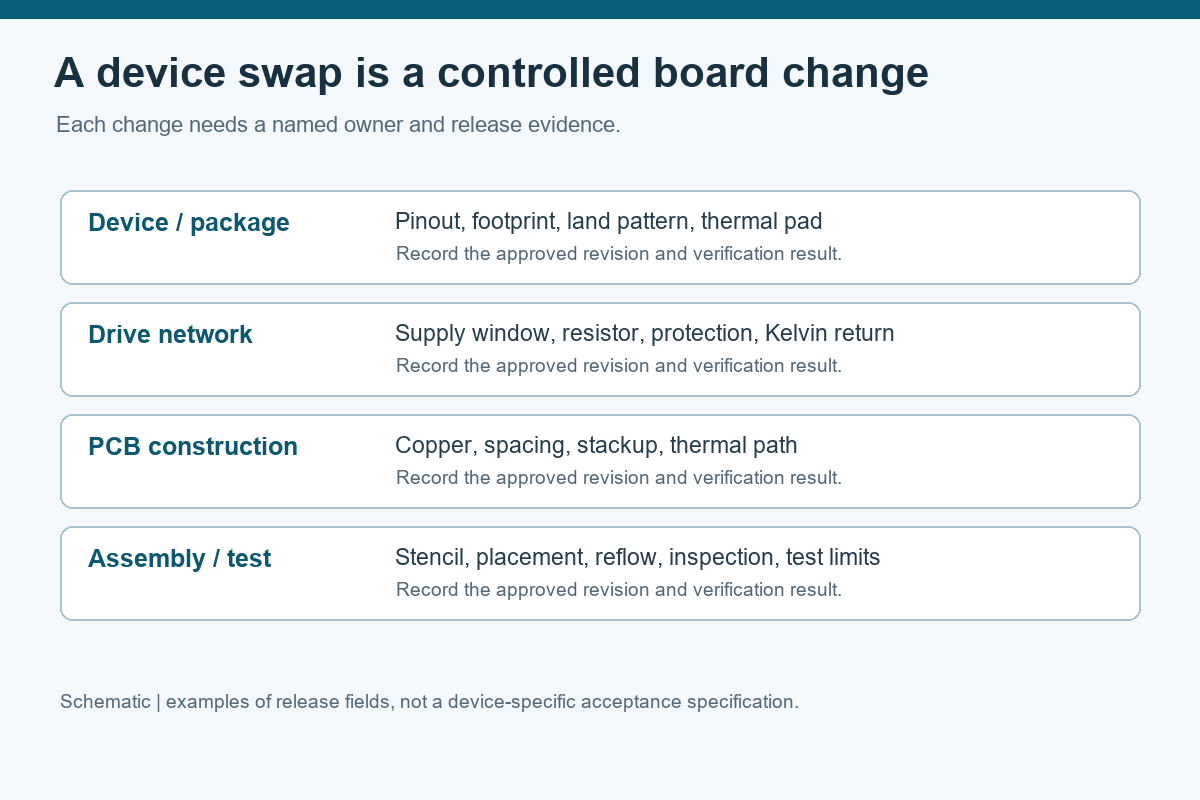
A part change can affect more than the device line on the BOM. The package and recommended land pattern can change paste deposition, component orientation, reflow compatibility, inspection visibility, heatsink fit, and the location of high-voltage spacing features. For a replacement part, compare its gate-drive limits, pinout, package dimensions, thermal interface and sourcing status before declaring it approved. Define these steps in the PCB assembly scope instead of assuming that a BOM change leaves the build process intact.
| Owner and record | Minimum release question | Hold if |
|---|---|---|
| Electrical design: device and driver | Are exact part numbers, gate limits, protection and operating assumptions frozen? | A substitute changes the pinout, drive window or fault response without review |
| PCB design: fabrication package | Do the land pattern, stackup, copper, spacing and return paths match the tested revision? | Layout or stackup differs from the tested build |
| Assembly engineering: process | Are stencil, placement, reflow, thermal-interface and inspection instructions defined? | Hidden joints or thermal-pad process lack an acceptance method |
| Test engineering: evidence | Are waveform, temperature, functional and protection checks linked to this revision? | Results belong to a different BOM, firmware or cooling setup |
| Procurement: sourcing | Are approved manufacturer part numbers, alternates and material terms explicit? | An unqualified alternate is treated as interchangeable |
This gate translates device selection into a reproducible build. A useful PCBA cost breakdown includes the package-dependent assembly and test work, not only the switch’s unit price. If the expected performance advantage requires a new layer stack, more inspection, or a different heat sink, include those costs in the same comparison.
What belongs in the quote and release package?
Send one controlled set of Gerbers or fabrication data, stackup and copper requirements, drill files, the approved BOM with manufacturer part numbers and alternates, placement data, assembly drawings, thermal-interface instructions, and a test outline. Add the operating bus, expected load, cooling setup, and any measured waveform or temperature limits that affect the build. State which items are engineering targets and which are production acceptance requirements.
The RFQ should also say whether devices are consigned or sourced by the assembler, whether selective inspection is required for the power package, and who owns fixture or heatsink installation. When candidates have different footprints, request separate cost and lead-time assumptions instead of collapsing them into one generic “SiC/GaN” quote.
If the design is ready for a build decision, provide the controlled fabrication and assembly package: files, BOM, placement data, thermal details, and test boundary. A combined PCB assembly quote should resolve the package process, material scope and verification plan against the chosen device revision.
The practical selection rule
Select the device and package that meet the real voltage, loss, fault and thermal requirements in a board that can be manufactured and verified. SiC and GaN offer different design opportunities, but the deciding evidence is a common-condition system comparison plus a controlled release package. Preserve the measured board revision and the assumptions behind the result; that prevents a promising laboratory switch from turning into an unrepeatable production build.
Technical references
- Texas Instruments, “Wide-bandgap semiconductors: Performance and benefits of GaN versus SiC” (2020; accessed October 22, 2026).
- Texas Instruments, “GaN Driver Schematic and Layout Recommendations” (2022; accessed October 22, 2026).
- Infineon, “GaN FETs: The gallium nitride power transistor” (accessed October 22, 2026).
Latest Blog
Contact Info
Phone: +86-755-82882936
Email: [email protected]
WhatsApp: +86-13570802455
Wechat: +86-13570802455
Address: 2nd floor,D Bldg.,Electric Link Technology Bldg.,Gongming,Guangming New Dist.,518106 Shenzhen, China