
Any-Layer HDI PCB: Prove the Routing Need Before an ELIC Build
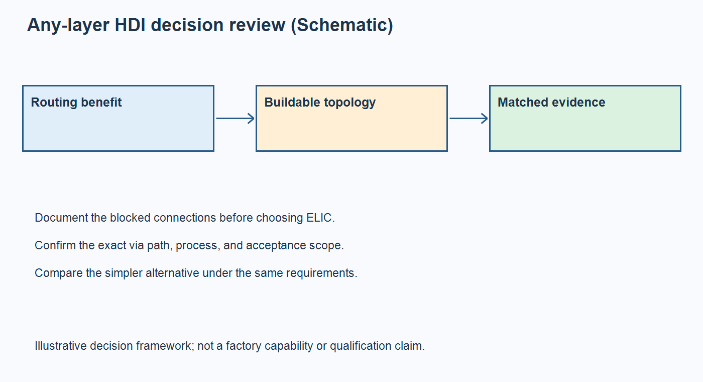
Table of Conent
Table of Conent
An any-layer HDI PCB is justified when a verified routing study needs microvia access throughout the stack, and a qualified fabrication process can support the resulting interconnect structure. Often called every layer interconnect (ELIC), this construction extends high-density connections beyond a limited outer build-up. It is not the default answer to a fine-pitch package, a high layer count, or an unfinished layout.
Make the decision with three records: a routing bottleneck log, a complete via topology, and evidence tied to the proposed construction and assembly exposure. Compare a simpler HDI option against the same electrical and mechanical requirements. The smaller board is useful only if its manufacturing, assembly, and qualification assumptions remain acceptable.
What does any-layer access change?
Any-layer access changes where a net can leave a package and reach another routing level. It does not remove capture pads, dielectric constraints, reference-plane requirements, or the manufacturing sequence.
In a conventional build-up, the available microvia spans may be concentrated near the outside of the board while a different structure connects deeper layers. An ELIC approach extends microvia interconnections throughout the stack. Altium’s ELIC explanation describes successive copper-filled microvia construction and the associated material and manufacturing constraints. Treat the finished connection as a sequence of approved transitions, not as an unrestricted hole between arbitrary layers.
Two paths can connect the same endpoints yet occupy different routing space and create different interfaces to manufacture. A stacked transition, a staggered transition with an intermediate trace, and a longer drilled connection are not interchangeable just because a netlist shows continuity. Show the actual intermediate pads and layers in the proposed topology.
For the broader package-escape workflow, use the HDI BGA escape and build-up release guide. The narrower question here is whether access throughout the stack produces a benefit that a more limited construction cannot deliver.
Prove the routing bottleneck before committing to ELIC
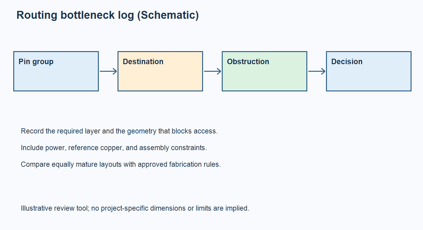
A useful routing proof identifies which connections fail in the simpler option and why. “The BGA is dense” is a starting observation, not a manufacturing requirement.
For each blocked pin group, record the required destination, allowed routing layers, pad and clearance assumptions, and the feature consuming the escape space. Include power and ground connections, reference copper, decoupling access, and any controlled-impedance constraints. A layer with empty geometric space may still be unsuitable because its reference arrangement or electrical role prevents the proposed route.
The TI Flip Chip BGA Package Reference Guide demonstrates that capture-pad geometry and trace/space choices change escape capacity. Its package examples support the method of checking geometry; their historical dimensions are not current universal manufacturing limits. Use the selected package drawing and the receiving fabricator’s reviewed rules.
Build a bottleneck log rather than comparing total unrouted-net counts alone. For example, distinguish a blocked inner row from a route that could be completed by moving a decoupling component or changing the permitted layer assignment. Repeat the comparison at similar placement maturity so that a polished ELIC layout is not being compared with an unfinished conventional one.
Choose the construction that resolves the documented constraint
Keep the simpler architecture when it meets the full requirement. Consider any-layer construction when access across the stack removes a documented constraint that remains after reasonable layout alternatives.
| Observed condition | Option to evaluate | Evidence needed |
|---|---|---|
| Only outer package rows need a short layer transition | Localized blind microvias or a limited build-up | Completed escape with approved geometry and reference paths |
| Several destinations remain inaccessible within the required outline | Any-layer/ELIC topology | Pin-group bottleneck log and complete proposed transition paths |
| Moving parts or increasing the outline resolves the conflict | Revised conventional or limited-HDI layout | Mechanical acceptance and a comparable routed layout |
| The proposed topology exceeds qualified process coverage | Redesign or qualify the specific construction | Documented fabrication review and an agreed qualification plan |
A routing benefit may be shorter lateral escape, reduced pad obstruction, or access to an otherwise unavailable layer. Record that benefit in the product’s own terms. Avoid translating it into an automatic signal-integrity improvement or a fixed percentage cost saving; those conclusions require analysis of the actual board and supplier quotation.
At this point, share the alternative stackups and blocked-connection map with the package drawing, draft fabrication data, BOM, placement file, quantities, and assembly requirements. Engineering can then review whether the proposed interconnect is supportable and which fabrication, sourcing, assembly, and testing assumptions need clarification before quotation.
Specify the full path, including its manufacturing dependencies
An ELIC specification should describe the finished interconnect and how the fabricator proposes to produce it. A layer-count label or the word “stacked” leaves too much unresolved.
Use a numbered cross-section and a via-span schedule. Identify the start and target layer of each microvia, the interfaces stacked on other features, the proposed dielectric construction, and the fill and surface condition. Distinguish an intermediate copper connection from a solderable outer land. The via-in-pad filling and capping guide addresses that assembly-facing surface; it does not replace a drawing of the internal ELIC path.
Ask the fabricator to identify the manufacturing sequence and the assumptions that drive registration, drilling, metallization, filling, and subsequent build-up. Do not derive a universal lamination-cycle count from the finished number of copper layers. The process route and starting construction must be confirmed. The PCB lamination review provides the material and press-control context.
Also identify what a proposed change would invalidate. A different material, via diameter, pad arrangement, fill process, or manufacturing site may require a fresh technical assessment even when the endpoints remain unchanged. Keep the approved topology with the supplier’s written responses, rather than allowing a quotation note to become an undocumented redesign.
Match reliability evidence to the construction you will buy
Qualification evidence should represent the actual interfaces and thermal exposure of the proposed board. General experience with HDI is useful background, but it does not establish every ELIC construction.
IPC’s March 2019 microvia reliability warning describes failures that can remain latent at room temperature and appear during reflow or later use. It also explains why conventional microsection inspection alone can miss some weak microvia interfaces. This is a reason to agree suitable evidence, not a claim that every stacked structure fails or that one universal stack-height limit applies.
Prepare an evidence-to-construction matrix. Link the proposed microvia chain to the sample or coupon that represents it, the material and process revision, the assembly exposure considered, the measurement method, the acceptance limits, and the responsible approver. Decide with the qualified fabricator and product owner which structures are representative or worst case. Do not assume the longest visible chain is the only important one.
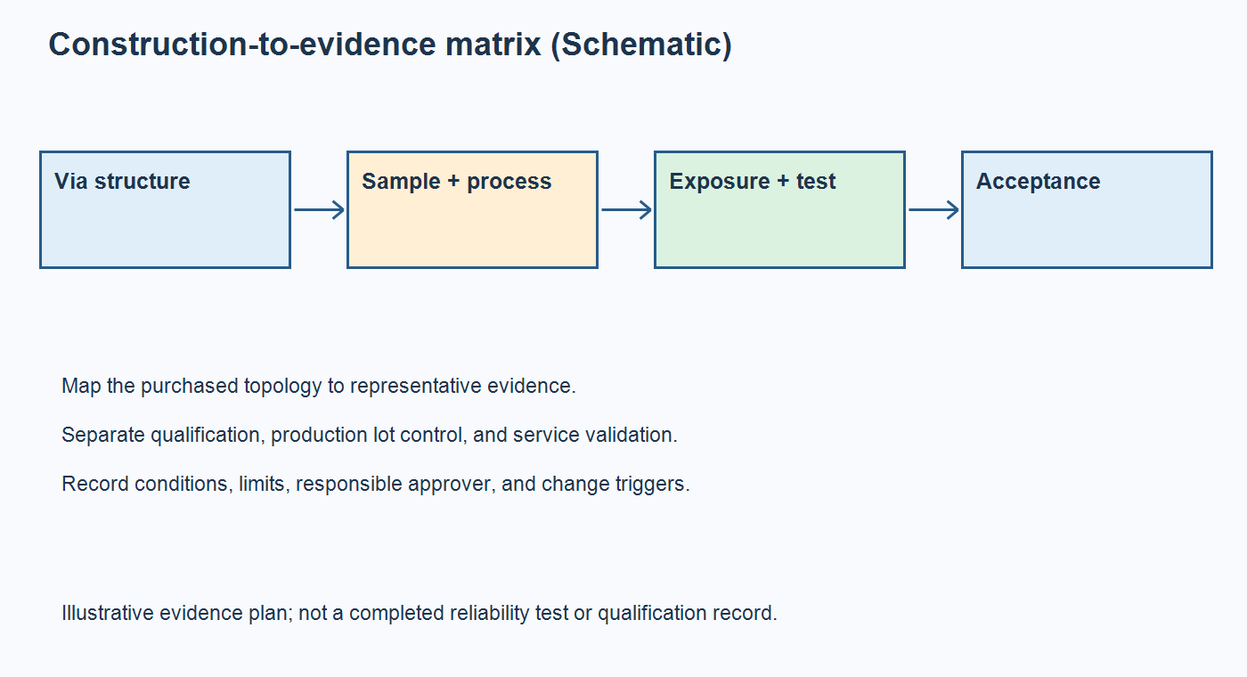
Separate qualification from routine lot control. A development experiment can investigate a risk without defining the final production acceptance method. Conversely, a production continuity check can confirm an agreed electrical condition without recreating the product’s service environment. Record what each result establishes and what remains outside its scope.
Assembly exposure belongs in the review: expected reflow passes, permitted rework, handling and moisture controls, and any later process affecting the board. Use the applicable product and manufacturing specifications to set conditions. Avoid borrowing test temperatures, resistance-change limits, or cycle counts from an unrelated paper and presenting them as a universal ELIC acceptance standard.
Keep optical inspection and buried-interface evidence separate
Assembly inspection and internal-interconnect evaluation address different defects. A surface inspection image cannot establish the integrity of a buried copper interface.
Plan inspection around the assembled product’s accessible features and hidden-joint risks, while keeping the fabrication acceptance plan tied to the internal construction. When a solderable land contains a microvia, agree the finished pad condition with stencil and reflow assumptions. Identify any test access that becomes unavailable after component placement, and decide when the relevant measurement must occur.
Compare quotes under one capability and acceptance boundary
Quotes are comparable only when they cover the same construction, assembly inputs, and evidence obligations. A low bare-board price can omit the work needed to establish an unfamiliar ELIC build.
Separate nonrecurring qualification or tooling from recurring board, component, assembly, inspection, and test costs. Record which assumptions remain conditional: material approval, panel arrangement, sample quantity, fixture ownership, documentation, or process changes. Ask how a prototype result will be transferred to the intended production process and which changes require reassessment.
A general HDI manufacturing service description is a starting point for discussion, not confirmation of an arbitrary every-layer topology. Project-specific feasibility must be established for the proposed stack and manufacturing route. Likewise, a full-turnkey PCB assembly scope should be tied to released fabrication data, sourcing rules, placement, and test requirements.
The release decision is to approve one construction with a documented routing benefit and an acceptable evidence plan. If the simpler option works, keep it in the comparison. When the complete project is ready for review, provide the controlled ELIC build package and acceptance matrix, including Gerber or ODB++ data, via spans, BOM, placement files, quantities, substitutions, and expected assembly exposure. The next step is to reconcile feasibility, sourcing, assembly, and qualification responsibilities before the build is priced or released.
Latest Blog
Contact Info
Phone: +86-755-82882936
Email: [email protected]
WhatsApp: +86-13570802455
Wechat: +86-13570802455
Address: 2nd floor,D Bldg.,Electric Link Technology Bldg.,Gongming,Guangming New Dist.,518106 Shenzhen, China