
UV Curing Controller PCB: Choose Vias for Current and Heat
Table of Conent
Table of Conent
A UV curing controller PCB should not use one via rule for every connection. The via structure must match the job: ordinary plated through vias can transfer load current between copper layers, a thermal-via array can move heat away from an exposed pad or UV LED mounting area, and filled-and-capped via-in-pad is justified only when routing density or the thermal interface requires it. The correct choice depends on continuous and pulsed current, allowable temperature rise, board thickness, copper distribution, assembly process, and the actual path from the heat source to the ambient environment.
The practical objective is not to maximize via count. It is to build a controlled electrical and thermal path that can be fabricated, assembled, inspected, and verified without creating solder loss, voiding, or unnecessary HDI cost.
Start with the current path and the heat path
Current and heat often share copper, but they are different design problems. A via used to move LED current from a top-layer driver circuit into an internal plane is part of the electrical series path. A cluster under a power package may carry little net load current while providing vertical thermal conduction into internal and bottom-side copper. The same physical hole can contribute to both functions, but it should not be sized by one shortcut.
Map the complete current loop before selecting vias. Include the input connector, protection components, switching device, inductor or linear pass element, current-sense resistor, LED output connector, and return path. Record continuous current, PWM duty cycle, transient current, copper thickness, and the maximum acceptable rise at the connector, copper, and via transitions. IPC-2152 describes current-carrying capacity as a relationship among current, conductor dimensions, board construction, environment, and acceptable temperature rise; it should be treated as a design framework rather than a universal “amps per via” table. The current IPC design standards list also includes IPC-2221 and IPC-2222 for general and rigid-board design requirements.
Then map the thermal path separately. Identify heat generated by the UV LEDs, LED driver, MOSFETs, rectifier, inductor, and sense resistor. Trace how heat reaches copper planes, the opposite PCB surface, a heat spreader, thermal interface material, enclosure, heatsink, and moving or still air. Nichia’s UV LED thermal guidance emphasizes that junction temperature depends on the selected LED, operating current, LED spacing, heatsink, and cooling structure, so the final assembly must be verified under its actual operating conditions.
Choose the via technology by function
The most economical solution is usually the least specialized via that satisfies the electrical, thermal, layout, and assembly requirements. Before specifying filled vias or microvias, determine whether conventional through vias plus adequate plane area already solve the problem.
Plated through vias for current transfer
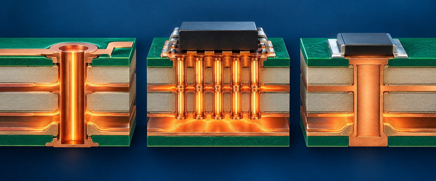
For a conventional multilayer controller, plated through vias are normally the first choice for transferring power between external and internal copper. Their effective resistance depends on finished hole diameter, plated barrel thickness, board thickness, copper connection geometry, and the number of vias sharing current. The entry and exit pads, thermal-relief pattern, neck-downs, and plane bottlenecks can dominate the result even when the barrel itself appears adequate.
Use multiple vias when the current, redundancy, or spreading requirement warrants it, but do not assume perfect current sharing. Unequal approach geometry can force the nearest via to carry more current. Arrange the vias across the width of the current path, connect them to solid copper on the relevant layers, and avoid routing a high-current transition through a thin thermal-relief spoke unless the connection has been evaluated for that load. Analog Devices likewise notes that via and track capability depends on plating, dimensions, routing layer, and operating temperature—not on a single nominal rating.
Thermal vias for vertical heat movement
Thermal vias connect a hot top-side copper region to internal planes, a bottom-side spreader, or a heatsink interface. Texas Instruments identifies via number, diameter, construction, and solder connection to the exposed pad as important variables, with diminishing returns as via copper area increases. More vias help only when they connect to copper that can continue moving heat.
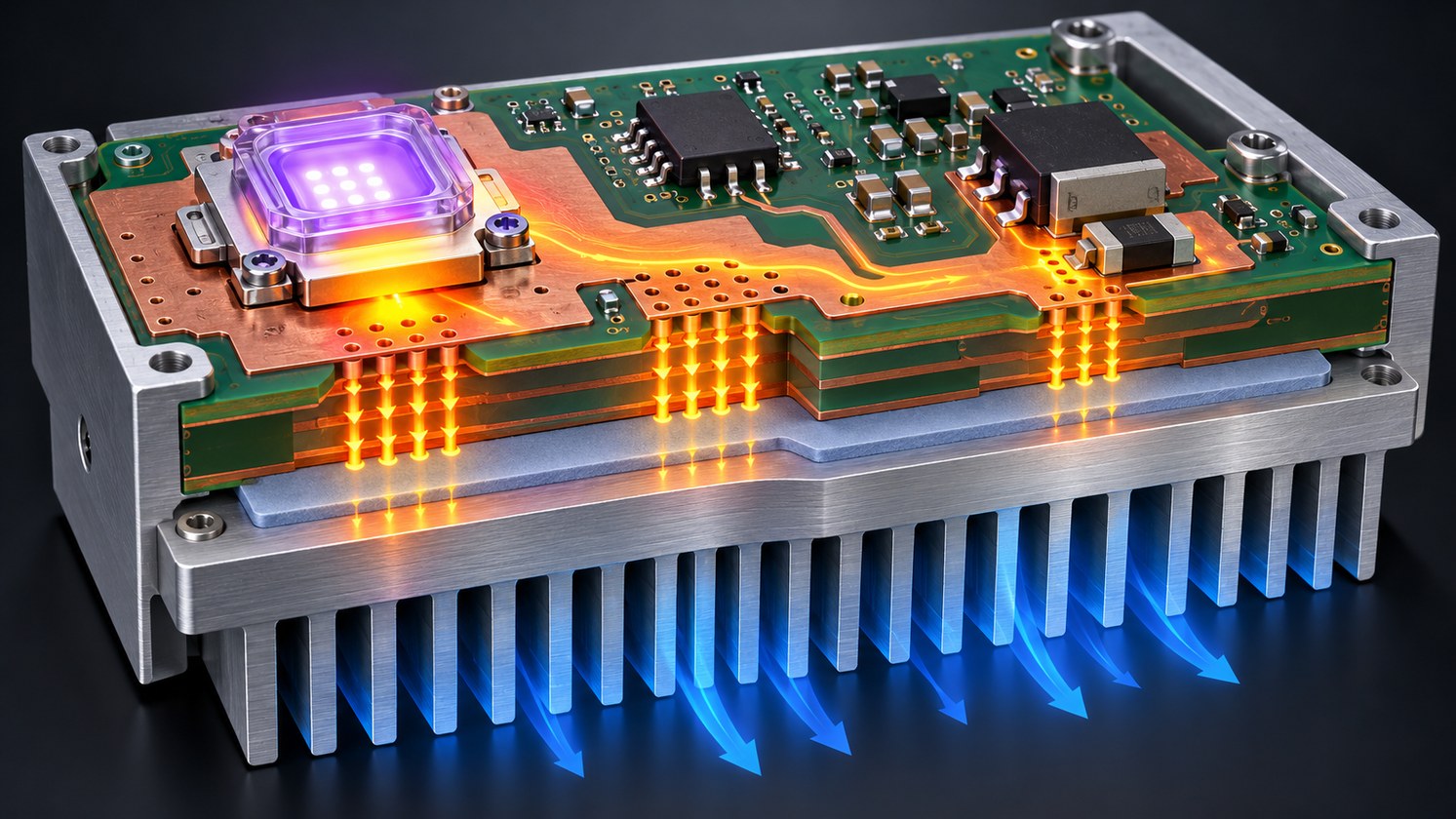
Keep the thermal path continuous. A dense array into a small isolated bottom pad can still trap heat. A modest array connected to a large internal plane, bottom copper, and a verified heat spreader may perform better. For UV LED modules, also consider thermal interference between adjacent emitters. Closely spaced heat sources can raise the local board and heatsink temperature even when each package has its own via array.
Via-in-pad, filled, and capped structures
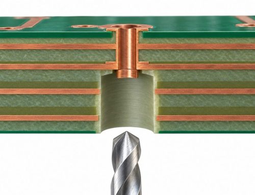
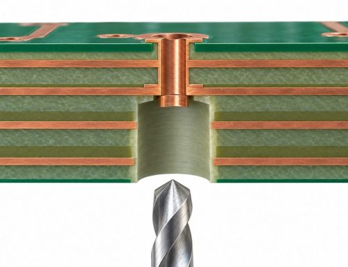
Via-in-pad can shorten the thermal path and release routing space, but an open via in a solderable pad can wick solder and reduce joint coverage. If the package land pattern requires vias inside the pad, define the filling, planarization, and capping requirement explicitly and confirm it with the fabricator. The via-in-pad filling and capping process must match the surface finish, flatness, and assembly inspection plan.
Do not specify filled-and-capped construction solely because it sounds thermally superior. Conductive fill can reduce part of the vertical thermal resistance, but cost, reliability, achievable aspect ratio, and manufacturing controls also change. In many controller sections, a conventional thermal-via array placed beside an exposed pad opening—or under the pad with an approved plugging process—provides the required performance at lower risk.
Separate the UV LED zone from the controller power zone
A UV curing system may place the LEDs on a metal-core board, ceramic substrate, or dedicated LED module while the controller uses an FR-4 PCB. That partition can simplify thermal management because the optical array and switching electronics have different placement, cooling, and service requirements. If the UV emitters share the controller PCB, the board stackup, copper weight, dielectric thickness, LED pitch, mechanical heat spreader, and assembly process must be designed together.
For the driver IC, MOSFET, and rectifier, follow the component manufacturer’s layout guidance. A TI LED-driver application report recommends a large ground pour under the driver, direct ground connection, thermal vias into additional copper layers, compact switching nodes, and careful separation of high-current paths from sensitive sense and timing nodes. Those details matter because a thermally strong layout can still produce unstable current or EMI if the switching loop is enlarged.
The LED current-sense path deserves special attention. Kelvin sense connections should not share uncontrolled voltage drop with the power return. Place the sense resistor and feedback routing according to the driver data sheet, keep sensitive traces away from switching copper, and document where the power current enters and leaves the sensing element. Vias in the sense path may be acceptable, but they must not obscure the intended sensing points.
If the design needs thick copper for low voltage drop or spreading, review the tradeoffs described for thick-copper PCB construction. Heavier copper affects etching, minimum geometry, thermal balance during assembly, hole plating expectations, and finished cost. It does not replace a complete heat path to the enclosure or heatsink.
When the power map, stackup, and cooling concept are ready, share the Gerbers, stackup, BOM, current table, and thermal interface drawing for an engineering review. This allows the fabrication, component sourcing, assembly, and thermal assumptions to be checked as one build package before tooling or prototype release.
Control solder, plugging, and inspection around thermal vias
Thermal performance depends on assembly quality. Open vias in or near a large exposed pad can pull solder away from the joint. Too much paste can float a package; too little can reduce thermal contact. The required mitigation may include tenting from one side, resin plugging, copper filling and capping, adjusted stencil apertures, or moving the via array outside the paste opening. The correct option depends on package geometry and the fabricator’s and assembler’s qualified processes.
ams OSRAM notes that the solder pad and stencil design influence joint reliability and heat dissipation for UV LEDs, and that void acceptance should be based on the application’s power dissipation and total thermal system rather than copied from an unrelated package rule. Define what will be inspected, how the result will be measured, and what constitutes acceptance. For hidden thermal pads, X-ray may be appropriate; for the complete thermal path, temperature measurement under representative operating conditions is still required.
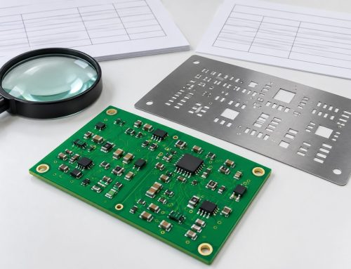
A clear assembly package should identify via treatment, solder-mask openings, paste layers, copper-filled features, flatness expectations, and any special inspection. Use a controlled PCB assembly drawing to communicate polarity, DNP rules, thermal interface materials, hardware torque, and test notes instead of relying on informal email instructions.
Verify the design with calculations and physical tests
Calculations are useful for screening alternatives, but the final UV curing assembly needs physical validation. TI’s thermal-conduction analysis shows how via barrel dimensions and material conductivity can be used to estimate vertical thermal resistance; it also notes that plating thickness depends on the board manufacturer and via geometry. Use actual fabrication assumptions, not a generic calculator default.
Build a verification plan around the real operating envelope:
- Measure input, LED, and switching currents at minimum, nominal, and maximum supply voltage.
- Exercise continuous output and the highest-energy PWM profile, including startup and fault recovery.
- Measure the driver, MOSFET, sense resistor, connector, LED solder point, PCB hot spots, heat spreader, and local ambient temperature.
- Test at the worst intended enclosure, airflow, orientation, contamination, and ambient condition.
- Confirm current regulation accuracy, UV output stability, thermal protection behavior, and recovery after cycling.
- Inspect exposed-pad and UV LED solder joints when the validation plan requires evidence of coverage or voiding.
Board thickness affects via length, aspect ratio, and the distance from hot components to bottom-side copper or a heat spreader. Review the electrical and mechanical consequences together when choosing PCB thickness and stackup tolerances. A thicker board can improve stiffness but lengthen the vertical thermal path and complicate small drilled features.
Release a buildable via specification
A useful fabrication note specifies finished hole or microvia geometry, pad size, copper plating expectation, layer connection, via fill or plug type, cap requirement, surface finish, solder-mask treatment, and applicable acceptance criteria. It should also identify which dimensions are design targets and which are controlled finished requirements. Avoid placing a generic “standard vias” note next to a thermal pad that actually needs a special process.
Before release, ask the PCB supplier to review aspect ratios, hole-to-copper spacing, annular ring, fill and cap capability, sequential-lamination needs, copper distribution, and coupon or inspection evidence. Then have the assembler review paste apertures, component stand-off, reflow compatibility, X-ray access, thermal interface installation, and test access. A documented PCB DFM review is most valuable when each issue is tied to a specific manufacturing risk and a controlled disposition.
Decision checklist
Use the following sequence instead of selecting vias from a generic ampacity chart:
- Define the continuous, pulsed, and fault current through each layer transition.
- Define the allowed voltage drop and temperature rise.
- Map every significant heat source and the complete path to ambient.
- Choose the simplest via construction that meets current, thermal, routing, and assembly needs.
- Confirm the stackup, copper weight, plating, via treatment, solder mask, and stencil plan with suppliers.
- Validate current sharing, temperatures, regulation accuracy, solder coverage, and protection behavior on representative hardware.
The right UV curing controller PCB may use several via strategies on the same board: parallel through vias for power transfer, thermal-via arrays for vertical spreading, and a limited number of filled-and-capped via-in-pad features where package density or heat flow justifies the added process. The selection is complete only when the electrical path, thermal path, fabrication notes, assembly controls, and validation evidence agree.
For a production review, provide the released Gerbers or ODB++, BOM, placement data, stackup, via notes, operating-current profiles, thermal limits, build quantity, and test requirements. OrinewPCB can then evaluate the PCB fabrication, component sourcing, assembly, and test scope against the same controlled design package.
References
Latest Blog

Contact Info
Phone: +86-755-82882936
Email: [email protected]
WhatsApp: +86-13570802455
Wechat: +86-13570802455
Address: 2nd floor,D Bldg.,Electric Link Technology Bldg.,Gongming,Guangming New Dist.,518106 Shenzhen, China