
PCB Silkscreen Design: Readable Markings and Release Checks
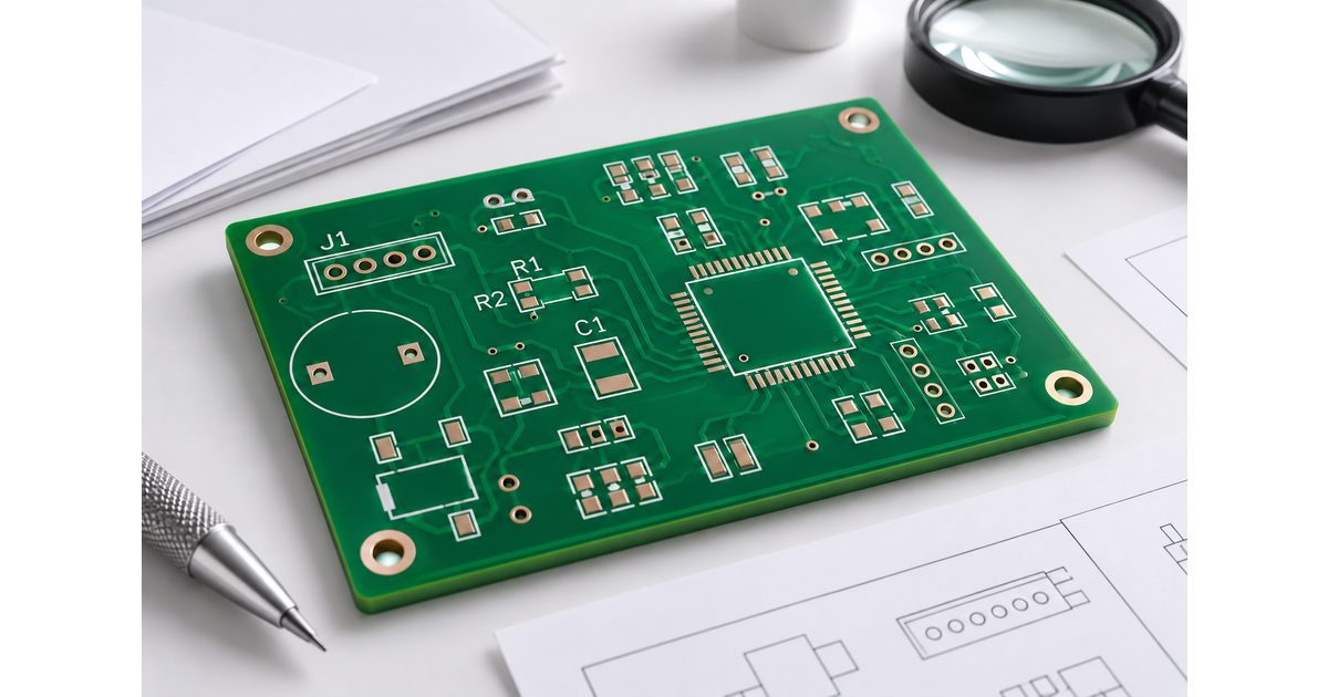
Table of Conent
Table of Conent
PCB silkscreen design should make the finished board easier to assemble, inspect, connect, and service. A reference designator that looks clear in the layout editor may become incomplete after manufacturing cleanup or disappear beneath a component. A polarity symbol that survives printing can still mislead the operator if its relationship to the device is ambiguous.
Treat the legend as functional information, not leftover decoration. Decide which markings must remain readable, keep them away from exposed soldering surfaces, and verify the exported top and bottom layers. This guide focuses on the decisions that prevent avoidable release problems without assuming a universal font size, ink process, or supplier clearance.
Start with what someone needs to identify
Divide the marking set by purpose. Assembly personnel need component references and orientation information. Test personnel may need connector identities and measurement-point labels. Service personnel need markings that remain visible after installation. Purchasing and configuration control may need a board identifier and a revision marking that agrees with the released documentation.
Prioritize information whose absence would create a genuine mistake. Keep a connector pin-one indication near the relevant end, make polarized-device orientation unambiguous, and distinguish neighboring references. A decorative logo should not push an essential label into a pad opening or leave the board revision too small to read.
For example, a densely populated sensor board might retain clear connector orientation and board identification on the physical legend while putting detailed component-location information in an assembly drawing. That is a hypothetical information-allocation decision, not permission to remove markings required by a customer specification. Resolve the actual requirement with the assembly and service teams.
Distinguish legend ink from copper and mask
The legend is normally printed information associated with a board surface; it does not define an electrical connection. Do not use a white outline as a substitute for a copper land pattern, a keepout rule, or an assembly drawing. Likewise, the mask color shown in a rendering does not establish how the selected ink will print.
Eurocircuits’ legend-print guidelines discuss separate legend data for each side, manufacturing clearances, and pre-production clipping. Its numerical limits and ordering workflow belong to that supplier. For another build, confirm the applicable process limits instead of copying them into a drawing as universal requirements.
Specify which sides require legend, the requested ink color if it matters, and any critical marking requirements. Do not infer that “white silkscreen” requires a particular screen-printing method. The supplier should confirm the process it proposes and whether it can reproduce the actual artwork.
Check the correct clearance boundary
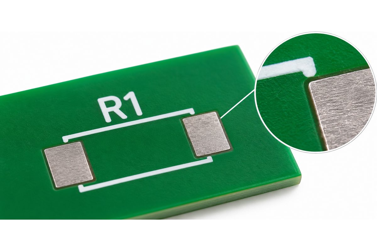
Keep legend away from soldering surfaces and other areas where ink is not intended. The relevant boundary may be exposed copper or the solder-mask opening, depending on the agreed manufacturing rule. Those boundaries are not always identical because the mask opening may extend beyond the copper feature.
Altium’s silk-to-mask clearance documentation distinguishes checks against exposed copper from checks against mask openings. That distinction explains why a layout can pass one rule yet need cleanup under a supplier’s interpretation. Configure the rule to match the production requirement and review the output.
The solder-mask openings and dams guide provides the related mask context. When an opening changes, nearby legend may need review even if the copper pad has not moved. Include exposed vias, test lands, holes, slots, and board-edge features rather than checking component pads alone.
Do not shrink a necessary mask opening just to rescue a text string. Move or redesign the marking, or use an agreed documentation alternative. A readable legend is valuable, but it should not compromise the soldering interface or another functional feature.
Design for the assembled board, not only the bare board
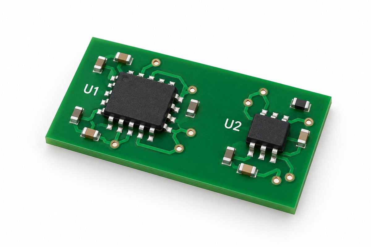
Place essential references where the installed component will not cover them. Compare the legend with component body outlines and assembly orientation, not only pad extents. A component can extend beyond its pads, and a connector housing can block a marking that was visible on the bare-board preview.
Review both sides separately. Bottom-side text should be checked using the intended viewing convention in the exported data. Do not manually mirror a layer merely because it appears reversed when overlaid from the opposite side; confirm how the CAD exporter and supplier interpret that side.
Keep each marking associated with the correct part. Moving R12 into free space is not helpful if it now appears to identify R13. For crowded areas, use a clear and consistent reference arrangement supported by the assembly drawing. Avoid long leader lines that cross unrelated features or become misleading after component substitutions.
If a critical marking is blocked, send the fabrication layers, assembly drawing, component body information, and marked visibility concerns for engineering review. Explain whether the label is needed during placement, test, or service so the proposed location can be assessed against its purpose.
Make polarity and orientation explicit
Use the component manufacturer’s package documentation and the approved footprint convention to establish orientation. A dot, stripe, plus sign, or pin-one marker should have a defined meaning. Do not assume every package uses the same polarity convention, or that an old library symbol remains correct after changing the part.
Check the legend against the schematic, footprint pin numbering, assembly drawing, and placement data. If two sources disagree, resolve the underlying design information before manufacture. Adding another symbol to the silkscreen can make the conflict harder to interpret rather than correcting it.
For connectors, identify the relevant end and function without crowding the mating or soldering area. Where a marking affects installation safety or product compliance, use the approved product requirements; a convenient PCB legend is not a substitute for the required labeling system.
Choose printable lettering without relying on one minimum
Text height alone does not determine legibility. Stroke width, spacing, character shape, contrast, printing resolution, and the underlying surface also matter. A narrow font can contain strokes that are too fine even when the overall character height seems generous.
Ask the supplier about minimum line width, minimum text height, spacing, and the treatment of marginal features. Use a practical margin where the layout allows it rather than designing every label exactly at a stated minimum. Evaluate the smallest punctuation and enclosed character details, not just a large sample letter.
Review the PCB manufacturing capabilities alongside the actual artwork, and request project-specific confirmation of critical legend details. General fabrication capability information does not prove a tiny text string or logo will remain readable after processing.
Review automatic clipping and movement
Manufacturing preparation can remove or trim legend that overlaps prohibited regions. That can protect a soldering area while damaging the meaning of a marking. A clipped polarity sign, a missing character, or an incomplete reference should be reviewed as an information problem, not merely a cosmetic change.
Altium’s silkscreen-preparation documentation describes automatic clipping and movement and the conditions under which objects can be removed or remain unresolved. Use such tools to identify problems, then inspect the changed artwork. Automatic clearance correction does not establish that the relocated text still points to the right component.
Preserve the original design and compare the prepared version before release. Review messages for unresolved objects and examine locked or excluded items. Confirm that the rule scope includes both requested legend sides and any panel-level markings that will be printed.
Need a supplier review before accepting cleanup? submit the legend and mask layers, highlighted essential markings, and proposed cleanup permissions for manufacturing review and quotation. State which labels must not be removed or repositioned without approval.
Verify exports and configuration information
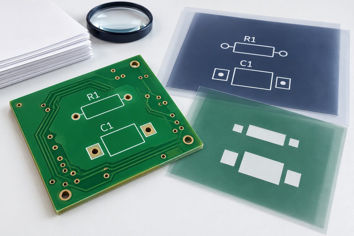
Export legend, copper, mask, drill, and outline data from one controlled revision. Open the exported package in an independent viewer and check the layer identities. The Gerber X2 release-check guide explains why file attributes and filenames should agree with the intended physical layers.
Compare top and bottom legend against the corresponding mask and outline. Look for absent references, unexpected mirrored text, clipped symbols, and markings outside the finished board. If the board is panelized, distinguish permanent product identification from rail information that will disappear during separation.
Keep assembly-only documentation separate from production legend. Do not accidentally export a mechanical or assembly layer full of notes as the printed overlay. Confirm that board identifiers, revision text, and any variable marking instructions match the purchasing package rather than an older template.
Pre-release checklist
- Identify required references, orientation marks, connector labels, and board identification.
- Check printability against the selected supplier’s process, not a generic minimum.
- Review clearance to the agreed mask or exposed-copper boundary, holes, and edges.
- Confirm markings remain meaningful and visible at their intended assembly or service stage.
- Compare automatic cleanup with the original artwork and resolve critical changes.
- Verify both exported legend sides and freeze one consistent revision.
Good PCB silkscreen design preserves useful information through fabrication and assembly. Place essential markings deliberately, use clear orientation conventions, and verify the manufactured-data interpretation. A clean layout preview is the starting point, not the final acceptance evidence.
Ready to order? submit the final fabrication package, assembly drawing, critical marking requirements, quantities, and revision information for engineering review and quotation. Include any unresolved legend changes before the order is released.
Latest Blog




Contact Info
Phone: +86-755-82882936
Email: [email protected]
WhatsApp: +86-13570802455
Wechat: +86-13570802455
Address: 2nd floor,D Bldg.,Electric Link Technology Bldg.,Gongming,Guangming New Dist.,518106 Shenzhen, China