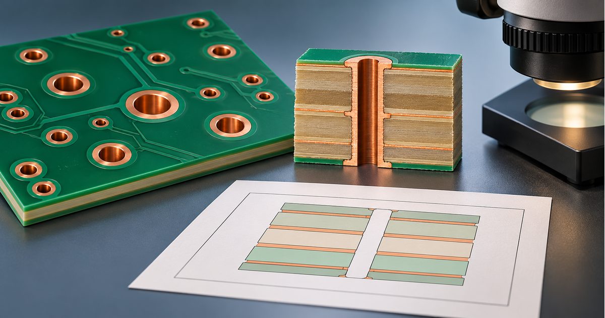
PCB aspect ratio describes how deep a hole is relative to its diameter. It is an important fabrication check because a deep, narrow opening presents different drilling and plating demands from a shallow, wide one.
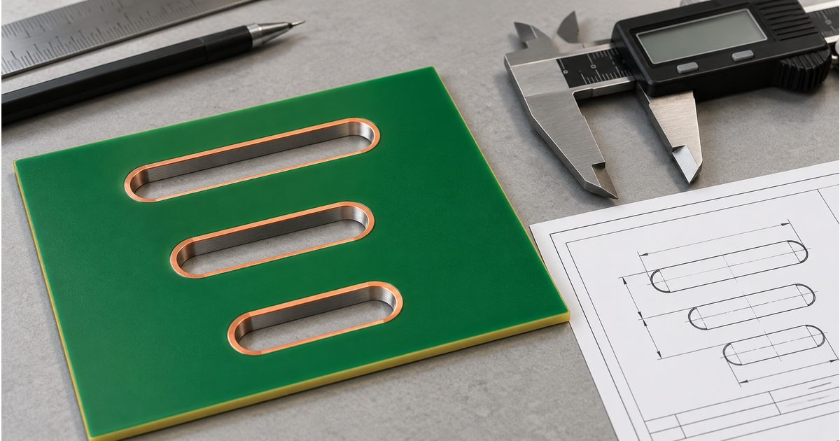
PCB slots accommodate features that do not fit a round hole, such as flat connector tabs, mechanical locating features, and selected board cut-outs. Their design involves more than drawing an oval. The fabricator needs to
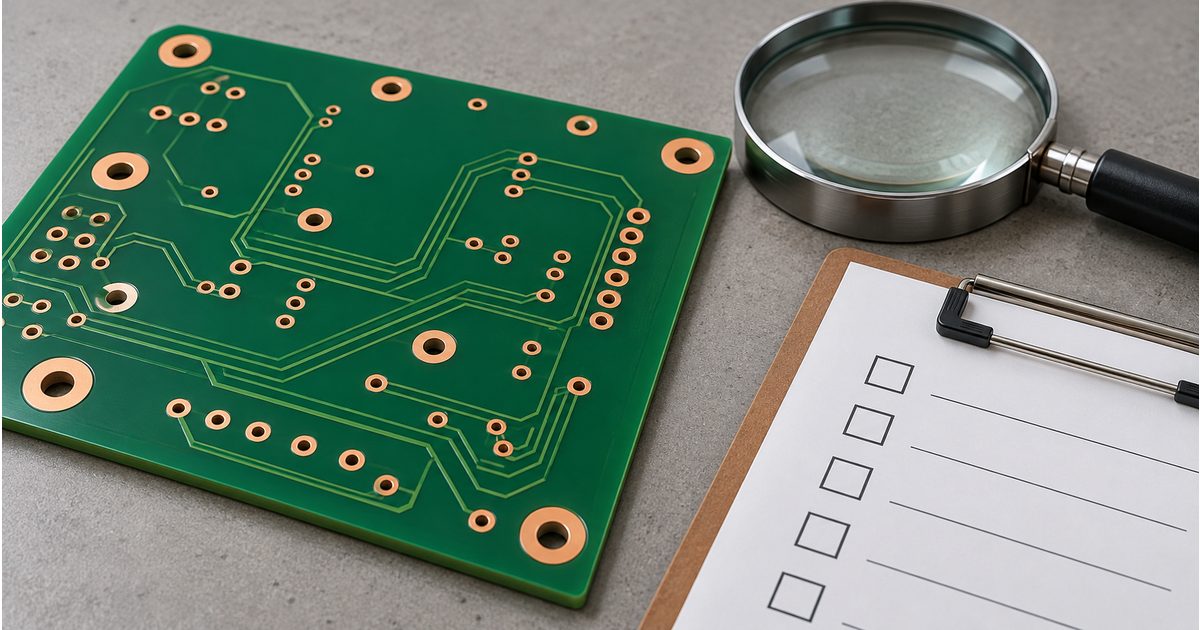
A PCB annular ring is the copper land surrounding a hole. It provides connection area at a via or plated-through-hole location, but its nominal width in CAD is not necessarily the narrowest width that remains
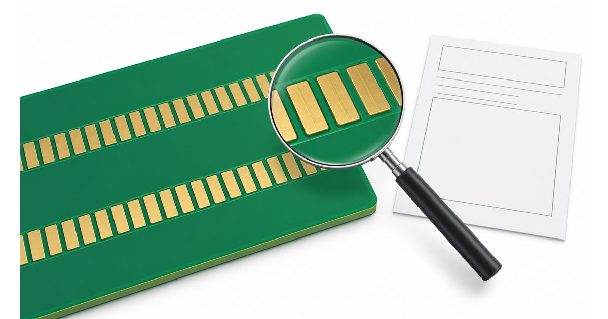
PCB solder mask design determines which copper areas remain exposed and where protective mask remains between features. A layout can have acceptable copper spacing yet produce unsuitable mask openings or fragile mask bridges. The practical
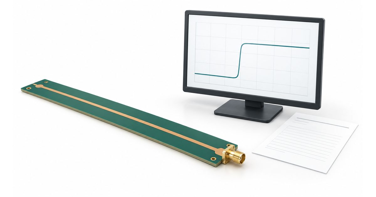
PCB impedance testing can confirm a defined transmission-line requirement, but an impedance number is only meaningful when it is tied to the right specimen and measurement conditions. A report should tell the buyer which structure
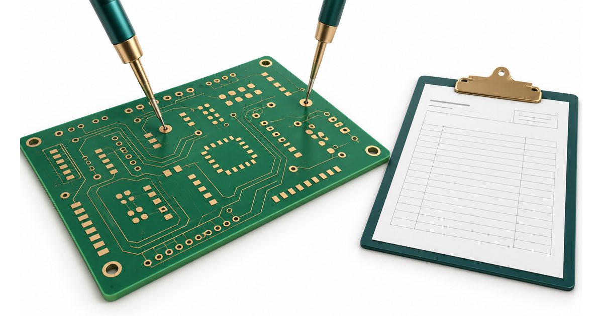
Bare-board PCB electrical testing checks a manufactured board's conductive networks before components are assembled. For a buyer, the key issue is not simply whether the shipment is marked “electrically tested.” It is whether the test
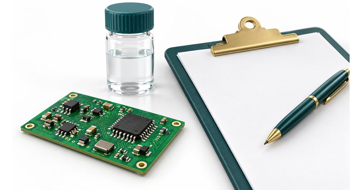
Ionic cleanliness testing for PCB assemblies is useful only when the result answers a defined manufacturing question. A number from a solvent extract can help monitor a process or investigate residues, but it does not
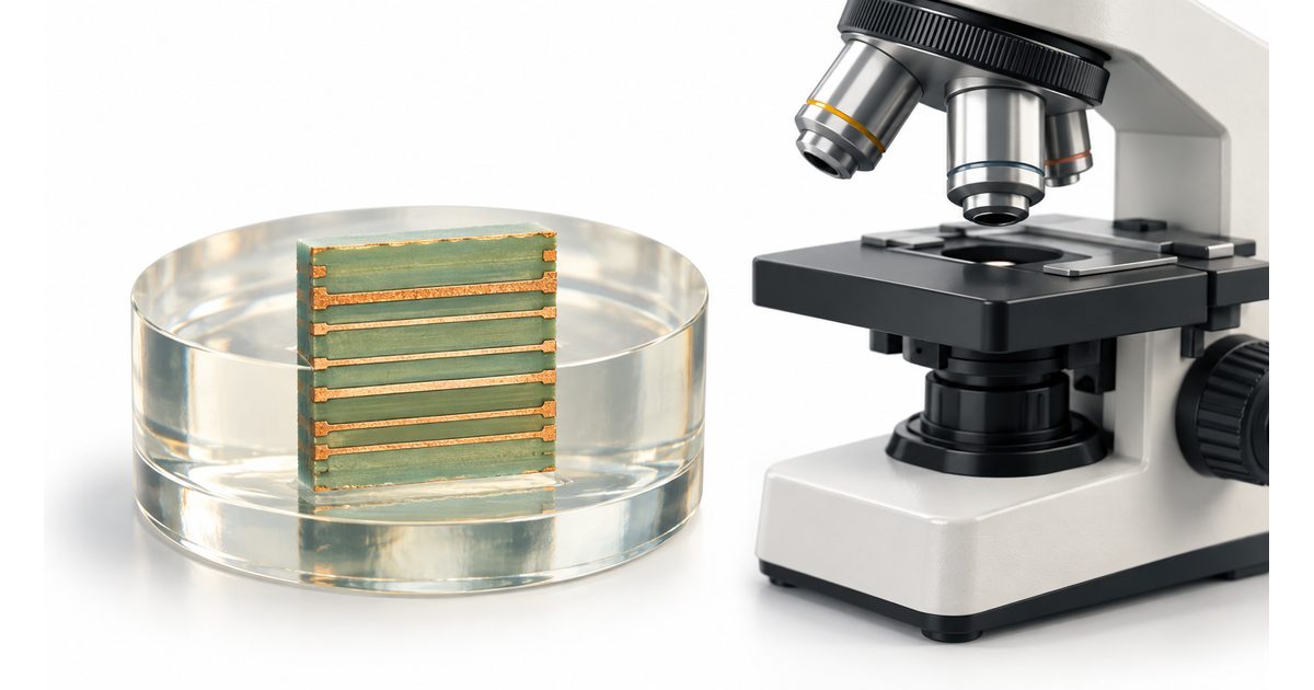
PCB microsection analysis exposes a selected internal plane so an engineer can inspect board construction and plated structures. It can support incoming acceptance, process qualification, or a failure investigation, but a convincing image is not
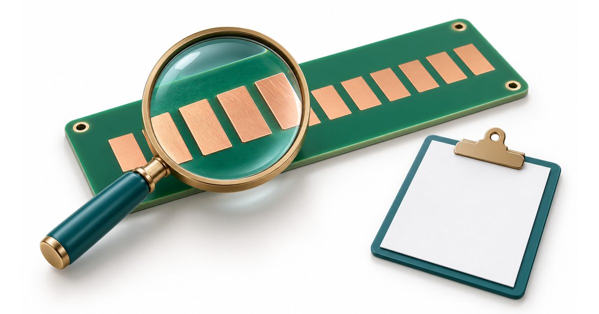
PCB solderability testing asks whether the specified board surface will wet with solder under defined conditions. It is useful when qualifying a surface finish, agreeing incoming inspection, investigating stored inventory, or separating a bare-board concern
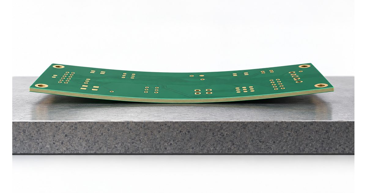
PCB bow and twist become purchasing problems when a board that looks acceptable on a desk will not print consistently, travel reliably through assembly equipment, or fit its enclosure without being forced. The useful question
Email us for a Free Quote: [email protected]
PCB MANUFACTURING & ASSEMBLY
Start your next PCB project
Share your requirements for PCB fabrication, assembly or component sourcing.

PCB fabrication, assembly and component sourcing — from prototype to production.
Orinew Technology Development Co., LTD.
Contact our team
Address17th Floor, 2B Bldg., Creative Bldg., Time Valley, Heshuikou Community, Matian Street, Guangming Dist., 518106 Shenzhen, China© 2012–2026 Orinew Technology Development Co., LTD.