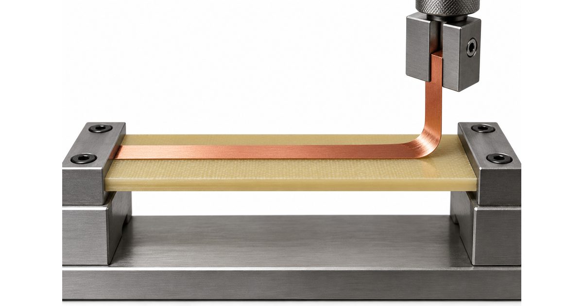
PCB peel strength testing evaluates the resistance of metallic cladding to separation from its laminate under a defined test method. For a copper-clad material, the result helps characterize the copper-to-laminate interface. It is meaningful only
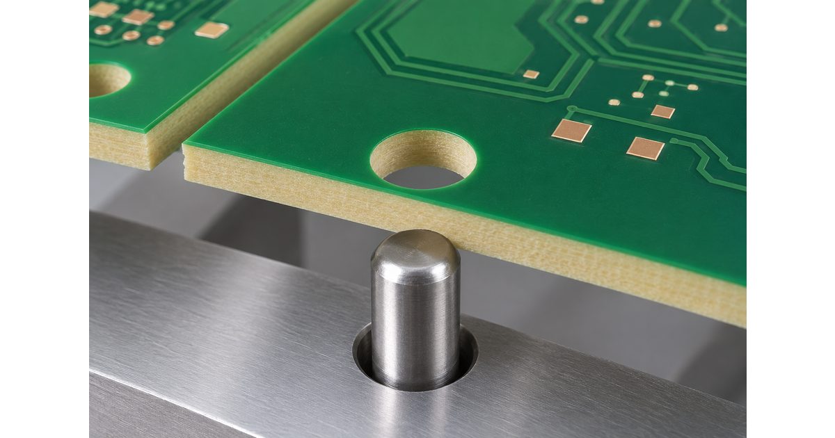
PCB tooling holes provide mechanical references for a manufacturing, assembly, or test fixture. Their usefulness depends on the hole geometry, location, mating locator, and the stage at which they are used. Adding an arbitrary hole
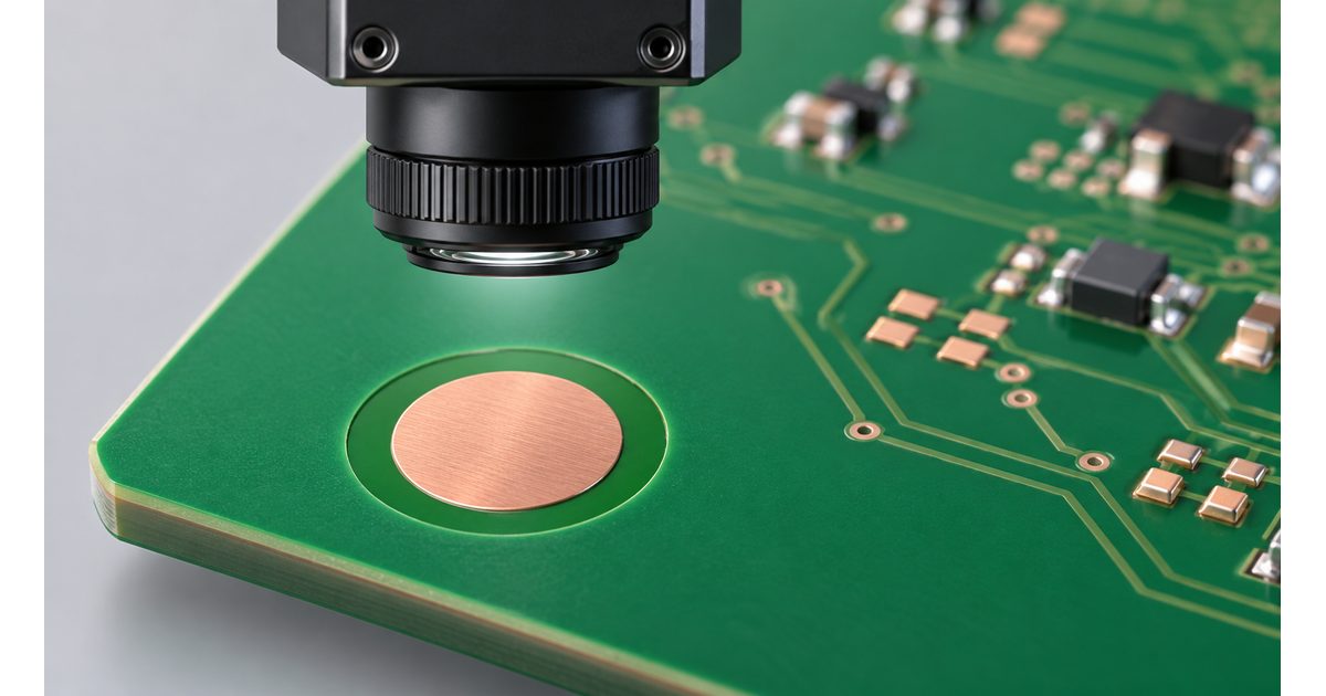
PCB fiducial marks give assembly equipment recognizable optical references on the board. The references help relate the physical PCB to the coordinates used for printing or component placement. A useful fiducial is a deliberately designed
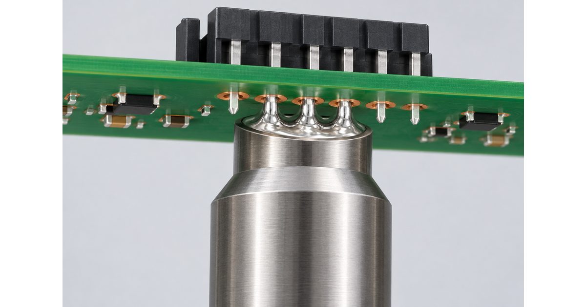
Selective soldering applies solder to designated locations instead of exposing the whole board underside to a conventional solder wave. For mixed-technology assemblies, a localized mini-wave process can join through-hole components while working around already assembled
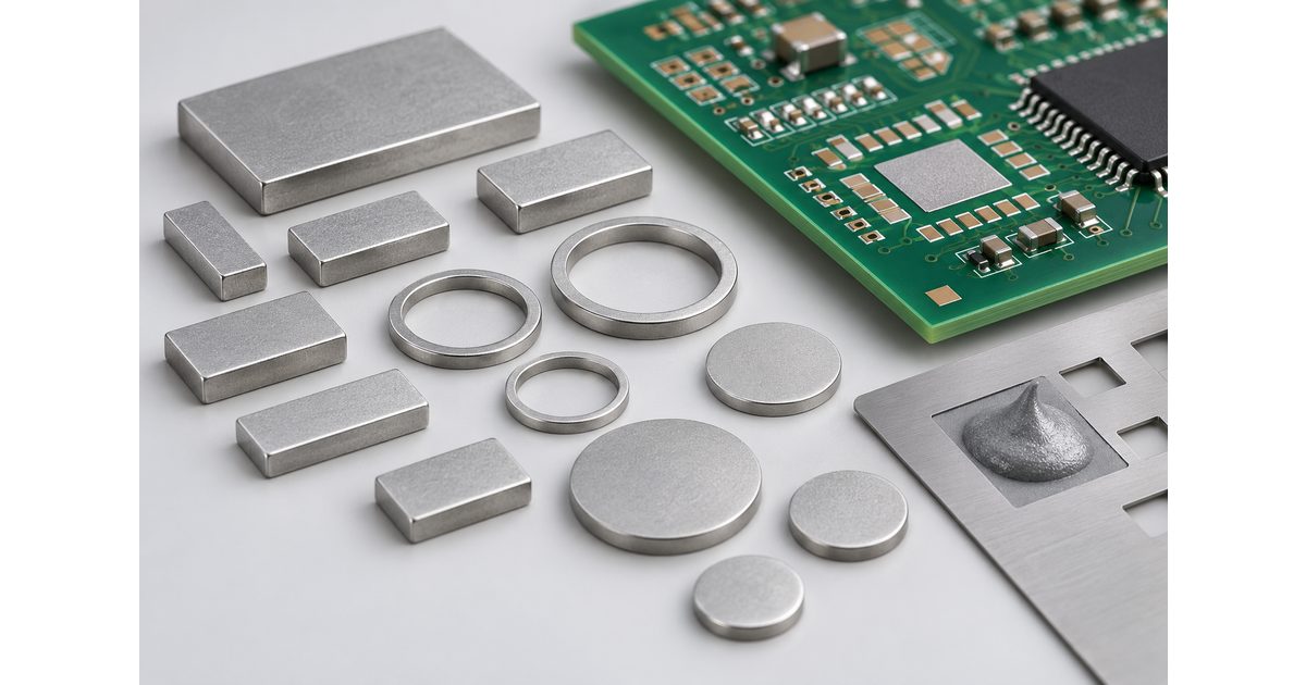
Solder preforms are solid pieces of solder alloy made in defined shapes and dimensions. They offer a way to place a controlled quantity of metal at a joint. In PCB assembly, a preform may supplement
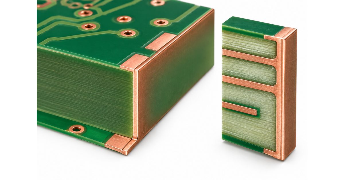
PCB edge plating adds a conductive metal coating to selected board sidewalls. It can provide a perimeter connection between specified copper layers or an interface to a shielding or contact arrangement. The design must define
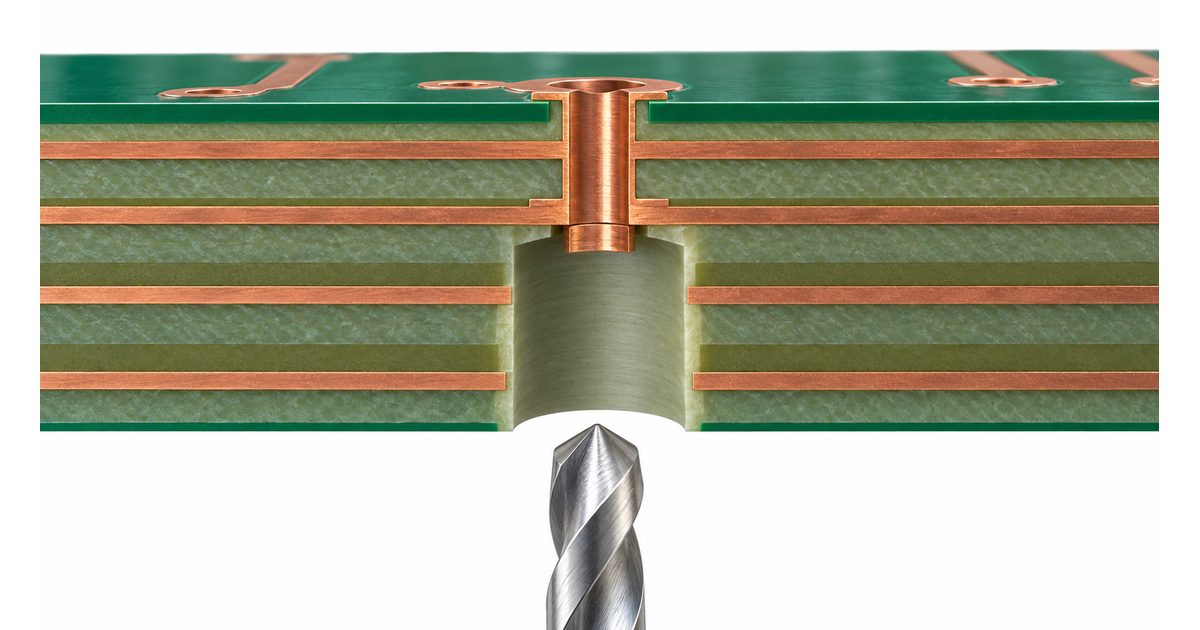
PCB backdrilling removes unwanted conductive barrel from a plated through-hole while preserving the part needed for the signal connection. It can help a high-speed channel when a via leaves an electrically significant unused stub. The
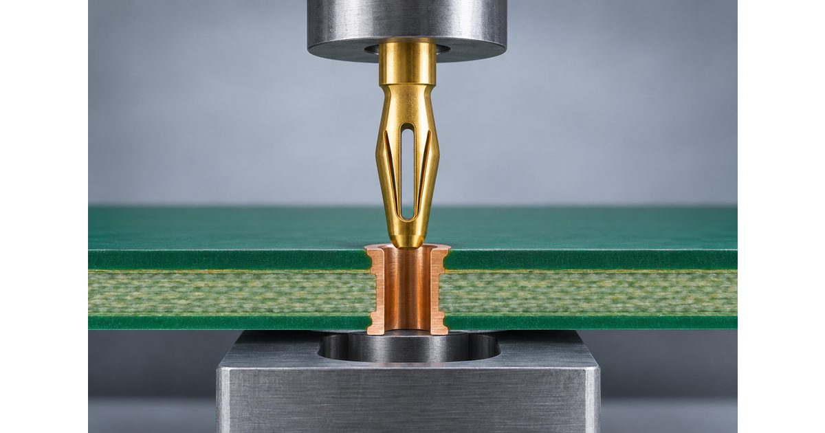
Press-fit PCB assembly joins a contact to a plated hole through a controlled insertion process. The connection depends on more than the connector part number: the finished hole, board construction, tooling, support, and seating conditions
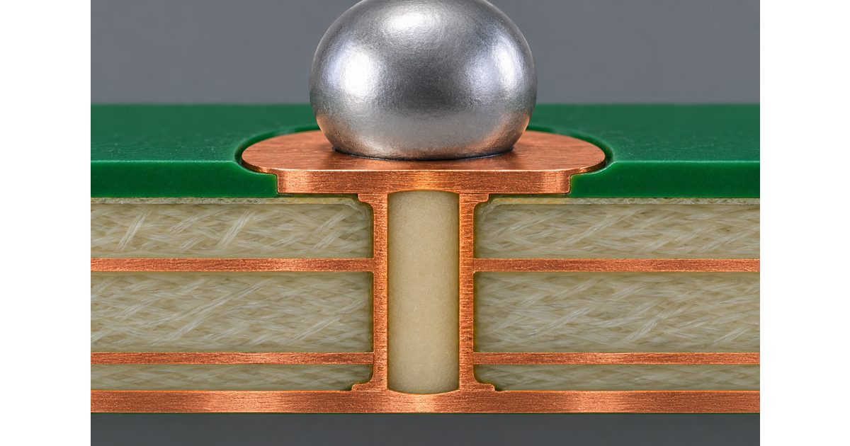
Via-in-pad places a via inside a component land instead of connecting the land to a separate via with a short trace. It can create valuable routing space around a dense package, but it also changes
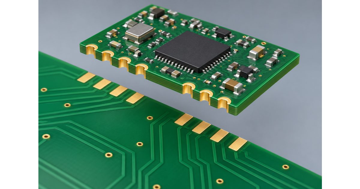
Castellated holes let a small PCB module connect to a larger host board through plated contacts along its edge. They can support a compact assembly without a separate header, but the module and host footprint
Email us for a Free Quote: [email protected]
PCB MANUFACTURING & ASSEMBLY
Start your next PCB project
Share your requirements for PCB fabrication, assembly or component sourcing.

PCB fabrication, assembly and component sourcing — from prototype to production.
Orinew Technology Development Co., LTD.
Contact our team
Address17th Floor, 2B Bldg., Creative Bldg., Time Valley, Heshuikou Community, Matian Street, Guangming Dist., 518106 Shenzhen, China© 2012–2026 Orinew Technology Development Co., LTD.